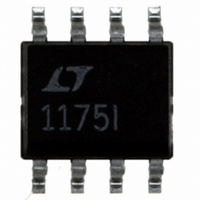
LT1175IS8#TRPBF Linear Technology, LT1175IS8#TRPBF Datasheet

LT1175IS8#TRPBF
Specifications of LT1175IS8#TRPBF
Available stocks
Related parts for LT1175IS8#TRPBF
LT1175IS8#TRPBF Summary of contents
Page 1
... Modems n Instrumentation n A/D and D/A Converters n Interface Drivers n Battery-Powered Systems L, LT, LTC, LTM, Linear Technology and the Linear logo are registered trademarks of Linear Technology Corporation. All other trademarks are the property of their respective owners. TYPICAL APPLICATION Typical LT1175 Connection + SHDN GND ...
Page 2
LT1175 ABSOLUTE MAXIMUM RATINGS Input Voltage (Transient 1 sec, Note 12) ...................25V Input Voltage (Continuous) .......................................20V Input-to-Output Differential Voltage (Note 13) ..........20V 5V SENSE Pin (with Respect to GND Pin) ......... 2V, –10V ADJ SENSE Pin (with Respect to OUTPUT ...
Page 3
... LT1175CN8-5#TRPBF LT1175CS8#PBF LT1175CS8#TRPBF LT1175CS8-5#PBF LT1175CS8-5#TRPBF LT1175CST-5#PBF LT1175CST-5#TRPBF LT1175CQ#PBF LT1175CQ#TRPBF LT1175CQ-5#PBF LT1175CQ-5#TRPBF LT1175CT#PBF LT1175CT#TRPBF LT1175CT-5#PBF LT1175CT-5#TRPBF LT1175IN8#PBF LT1175IN8#TRPBF LT1175IN8-5#PBF LT1175IN8-5#TRPBF LT1175IS8#PBF LT1175IS8#TRPBF LT1175IS8-5#PBF LT1175IS8-5#TRPBF LT1175IST-5#PBF LT1175IST-5#TRPBF LT1175IQ#PBF LT1175IQ#TRPBF LT1175IQ-5#PBF LT1175IQ-5#TRPBF LT1175IT#PBF LT1175IT#TRPBF LT1175IT-5#PBF LT1175IT-5#TRPBF LT1175MPS8#PBF LT1175MPS8#TRPBF LT1175MPS8-5#PBF LT1175MPS8-5#TRPBF LT1175MPQ#PBF LT1175MPQ#TRPBF LT1175MPQ-5#PBF LT1175MPQ-5#TRPBF ...
Page 4
LT1175 ORDER INFORMATION LEAD FREE FINISH TAPE AND REEL LT1175IT LT1175IT#TR LT1175IT-5 LT1175IT-5#TR LT1175MPS8 LT1175MPS8#TR LT1175MPS8-5 LT1175MPS8-5#TR LT1175MPQ LT1175MPQ#TR LT1175MPQ-5 LT1175MPQ-5#TR Consult LTC Marketing for parts specifi ed with wider operating temperature ranges. *The temperature grade is identifi ...
Page 5
ELECTRICAL CHARACTERISTICS temperature range, otherwise specifi cations are avoid confusion with “min” and “max” as applied to negative voltages, all voltages are shown as absolute values except where polarity is not obvious. PARAMETER Current Limit (Note 12) ...
Page 6
LT1175 TYPICAL PERFORMANCE CHARACTERISTICS Typical Current Limit Characteristics 1.0 CURRENT LIMIT CHANGES ONLY SLIGHTLY WITH TEMPERATURE SO CURVES ARE REPRESENTATIVE OF ALL TEMPERATURES 0 TIED TO V LIM2 LIM4 IN 0.6 I TIED TO V LIM4 IN ...
Page 7
TYPICAL PERFORMANCE CHARACTERISTICS Shutdown Input Current 25° 125° –55° INPUT VOLTAGE (V) 1175 G07 GND Pin Current ...
Page 8
LT1175 PIN FUNCTIONS (N8/Q/ST/S8/T) V (Pins 1, 8/Pin 3, Tab/Pin 2, Tab/Pins 1, 8/Pin 3, Tab): IN Power is supplied to the device through this pin. A bypass capacitor is required on this pin if the device is more than ...
Page 9
APPLICATIONS INFORMATION Note to Reader: To avoid confusion when working with negative voltages (is –6V more or less than –5V?), I have decided to treat the LT1175 were a positive regulator and express all voltages as positive ...
Page 10
LT1175 APPLICATIONS INFORMATION normally a good thing when the regulator is used by itself, but it prevents the user from shutting down the regulator when a second power source is connected to the LT1175 output. If active output pull-down is ...
Page 11
APPLICATIONS INFORMATION LT1175 AC FEEDFORWARD PATH NEGATIVE DC FEEDBACK Q3 AT LIGHT LOADS This condition can occur with ceramic or fi lm capacitors which often have an ESR under 0.1Ω. With previous de- signs, the user was forced to add ...
Page 12
LT1175 APPLICATIONS INFORMATION capacitors do not fail during a “shorting out” surge, only during a “charge up” surge. The output capacitor should be located within several inches of the regulator. If remote sensing is used, the output capacitor can be ...
Page 13
... Input Voltage Lower Than Output Linear Technology’s positive low dropout regulators LT1121 and LT1129, will not draw large currents if the input voltage is less than the output. These devices use a lateral PNP power transistor structure that has 40V emitter base breakdown voltage ...
Page 14
LT1175 APPLICATIONS INFORMATION To estimate regulator output ripple under different conditions, the following general comments should be helpful: 1. Output ripple at high frequency is only weakly affected by load current or output capacitor size for medium to heavy loads. ...
Page 15
PACKAGE DESCRIPTION .300 – .325 (7.620 – 8.255) .008 – .015 (0.203 – 0.381) +.035 .325 –.015 ( +0.889 8.255 –0.381 NOTE: 1. DIMENSIONS ARE *THESE DIMENSIONS DO NOT INCLUDE MOLD FLASH OR PROTRUSIONS. MOLD FLASH OR PROTRUSIONS SHALL NOT ...
Page 16
LT1175 PACKAGE DESCRIPTION .060 .256 (1.524) (6.502) .060 .183 (1.524) (4.648) .075 (1.905) .300 (7.620) BOTTOM VIEW OF DD PAK HATCHED AREA IS SOLDER PLATED COPPER HEAT SINK .067 RECOMMENDED SOLDER PAD LAYOUT NOTE: 1. DIMENSIONS IN INCH/(MILLIMETER) 2. DRAWING ...
Page 17
PACKAGE DESCRIPTION .245 MIN .030 ±.005 TYP RECOMMENDED SOLDER PAD LAYOUT .010 – .020 (0.254 – 0.508) .008 – .010 (0.203 – 0.254) NOTE: 1. DIMENSIONS IN 2. DRAWING NOT TO SCALE 3. THESE DIMENSIONS DO NOT INCLUDE MOLD FLASH ...
Page 18
LT1175 PACKAGE DESCRIPTION .390 – .415 (9.906 – 10.541) .230 – .270 (5.842 – 6.858) .460 – .500 (11.684 – 12.700) .330 – .370 (8.382 – 9.398) .067 BSC .028 – .038 (1.70) (0.711 – 0.965 Package 5-Lead ...
Page 19
... Replaced Note 2, renumbered all other notes and revised shutdown thresholds in the Electrical Characteristics section. Updated Related Parts. Information furnished by Linear Technology Corporation is believed to be accurate and reliable. However, no responsibility is assumed for its use. Linear Technology Corporation makes no representa- tion that the interconnection of its circuits as described herein will not infringe on existing patent rights. LT1175 ...
Page 20
... SOT-223, 8-Lead SO, TO-92 Packages DD-Pak, SOT-223, 8-Lead SO, TO-220, 20-Lead TSSOP Packages DD-Pak, TO-220 Packages SOT-223, 8-Lead SO, 8-Lead MSOP Packages DD-Pak, TO-220 Packages 5-Lead TSOT-23, 8-Lead (3mm × 3mm) DFN Packages www.linear.com ● 1175ff LT 0710 REV F • PRINTED IN USA © LINEAR TECHNOLOGY CORPORATION 1995 ...


