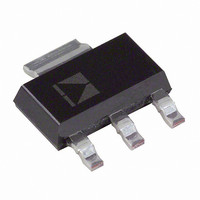
ADP3338AKCZ-3.3RL7 Analog Devices Inc, ADP3338AKCZ-3.3RL7 Datasheet - Page 10

ADP3338AKCZ-3.3RL7
Manufacturer Part Number
ADP3338AKCZ-3.3RL7
Description
IC REG LDO 1A PREC 3.3V SOT-223
Manufacturer
Analog Devices Inc
Series
anyCAP®r
Datasheet
1.ADP3338AKCZ-5-R7.pdf
(16 pages)
Specifications of ADP3338AKCZ-3.3RL7
Regulator Topology
Positive Fixed
Voltage - Output
3.3V
Voltage - Input
Up to 8V
Voltage - Dropout (typical)
0.19V @ 1A
Number Of Regulators
1
Current - Output
1A
Operating Temperature
-40°C ~ 85°C
Mounting Type
Surface Mount
Package / Case
SOT-223 (3 leads + Tab), SC-73, TO-261
Primary Input Voltage
8V
Output Voltage Fixed
3.3V
Dropout Voltage Vdo
190mV
No. Of Pins
3
Output Current
1A
Operating Temperature Range
-40°C To +85°C
Msl
MSL 3 - 168 Hours
Voltage Regulator Case Style
SOT-223
Rohs Compliant
Yes
Lead Free Status / RoHS Status
Lead free / RoHS Compliant
Current - Limit (min)
-
Lead Free Status / RoHS Status
Lead free / RoHS Compliant, Lead free / RoHS Compliant
Other names
ADP3338AKCZ-3.3RL7TR
ADP3338
APPLICATION INFORMATION
CAPACITOR SELECTION
Output Capacitor
The stability and transient response of the LDO is a function of
the output capacitor. The ADP3338 is stable with a wide range
of capacitor values, types, and ESR (anyCAP). A capacitor as
low as 1 µF is the only requirement for stability. A higher ca-
pacitance may be necessary if high output current surges are
anticipated, or if the output capacitor cannot be located near the
output and ground pins. The ADP3338 is stable with extremely
low ESR capacitors (ESR ≈ 0) such as multilayer ceramic capacitors
(MLCC) or OSCON. Note that the effective capacitance of some
capacitor types falls below the minimum over temperature or
with dc voltage.
Input Capacitor
An input bypass capacitor is not strictly required, but is recom-
mended in any application involving long input wires or high
source impedance. Connecting a 1 µF capacitor from the input
to ground reduces the sensitivity of the circuit to PC board
layout and input transients. If a larger output capacitor is
necessary, a larger value input capacitor is recommended.
OUTPUT CURRENT LIMIT
The ADP3338 is short-circuit protected by limiting the pass
transistor’s base drive current. The maximum output current is
limited to approximately 2 A (see Figure 16).
THERMAL OVERLOAD PROTECTION
The ADP3338 is protected against damage due to excessive
power dissipation by its thermal overload protection circuit.
Thermal protection limits the die temperature to a maximum of
160°C. Under extreme conditions, such as high ambient
temperature and power dissipation where the die temperature
starts to rise above 160°C, the output current is reduced until
the die temperature has dropped to a safe level.
Current and thermal limit protections are intended to protect
the device against accidental overload conditions. For normal
operation, externally limit the power dissipation of the device
so the junction temperature does not exceed 150°C.
Rev. B | Page 10 of 16
CALCULATING POWER DISSIPATION
Device power dissipation is calculated as
Where I
V
Assuming the worst-case operating conditions are I
I
dissipation is
So, for a junction temperature of 125°C and a maximum
ambient temperature of 85°C, the required thermal resistance
from junction to ambient is
PRINTED CIRCUIT BOARD LAYOUT
CONSIDERATIONS
The thermal resistance, θ
sum of the junction-to-case and the case-to-ambient thermal
resistances. The junction-to-case thermal resistance, θ
determined by the package design and is specified at 26.8°C/W.
However, the case-to-ambient thermal resistance is determined
by the printed circuit board design.
As shown in Figure 22, the amount of copper to which the
ADP3338 is mounted affects thermal performance. When
mounted to the minimal pads of 2 oz. copper, as shown in
Figure 22 (a), θ
under the ADP3338, as shown in Figure 22 (b), reduces the θ
102.9°C/W. Increasing the copper pad to one square inch, as
shown in Figure 22 (c), reduces the θ
GND
IN
and V
= 10 mA, V
P
P
θ
D
D
JA
a
= (V
= (3.3 V – 2.5 V) × 1000 mA + (3.3 V × 10 mA) = 833 mW
LOAD
=
OUT
125
IN
and I
are the input and output voltages, respectively.
. 0
– V
°
JA
C
833
IN
is 126.6°C/W. Adding a small copper pad
GND
OUT
−
= 3.3 V, and V
85
W
) × I
are load current and ground current, and
b
°
Figure 22. PCB Layouts
C
LOAD
JA
=
, of the SOT-223 is determined by the
48
+ (V
°
C/W
OUT
IN
JA
× I
= 2.5 V, the device power
even further to 52.8°C/W.
GND
)
c
LOAD
JC
, is
= 1.0 A,
JA
to


