NCP630AD2TR4G ON Semiconductor, NCP630AD2TR4G Datasheet
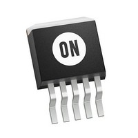
IC REG LDO 3A ADJ VOLT D2PAK-5

NCP630AD2TR4G

Manufacturer Part Number
NCP630AD2TR4G
Description
IC REG LDO 3A ADJ VOLT D2PAK-5
Manufacturer
ON Semiconductor
Datasheet

Specifications of NCP630AD2TR4G

Regulator Topology
Positive Adjustable
Voltage - Output
Adjustable
Voltage - Input
Up to 12V
Voltage - Dropout (typical)
1V @ 3A
Number Of Regulators
1
Current - Output
3A
Current - Limit (min)
3A
Operating Temperature
-40°C ~ 125°C
Mounting Type
Surface Mount
Package / Case
TO-263-5, D²Pak (5 leads + Tab), TO-263BA
Number Of Outputs
1
Polarity
Positive
Input Voltage Max
12 V
Output Type
Adjustable
Dropout Voltage (max)
1 V at 300 mA
Output Current
3 A
Line Regulation
0.02 %
Load Regulation
0.01 %
Voltage Regulation Accuracy
1.5 %
Maximum Operating Temperature
+ 125 C
Mounting Style
SMD/SMT
Minimum Operating Temperature
- 40 C
Reference Voltage
1.234 V
Lead Free Status / RoHS Status
Lead free / RoHS Compliant
Other names
NCP630AD2TR4G
NCP630AD2TR4GOSTR

Available stocks

Company
Part Number
Manufacturer
Quantity
Price
Part Number:
NCP630AD2TR4G
Manufacturer:
ON/安森美
Quantity:
20 000
NCP630
3.0 A Fast Linear Voltage
Regulators
capable of providing a guaranteed output current of 3.0 A with a
maximum dropout voltage of 1.25 V at 3.0 A over temperature. The
fast turn on time allows step changes in loads commonly found in low
voltage microprocessor applications. The NCP630 is currently offered
as an adjustable output version that can be programmed down to 1.2 V
with two external resistors and as a fixed output version at 3.47 V. On
chip trimming adjusts the reference/output voltage to within "1.5%
accuracy. Internal protection features consist of output current limiting
and thermal shutdown. NCP630 is available in D
Features
Applications
INPUT
© Semiconductor Components Industries, LLC, 2005
June, 2005 − Rev. 5
R2 + R1
The NCP630 is a low dropout positive voltage regulator that is
68 mF −
Output Current of 3.0 A
1.25 V Maximum Dropout Voltage at 3.0 A Over Temperature
Voltage on Shutdown Pin is TTL Compatible
Reference/Output Voltage Trimmed to "1.5%
Current Limit Protection
Thermal Shutdown Protection
−40°C to 125°C Junction Temperature Range
Pb−Free Packages are Available
Microprocessor Power Supplies
DSP Power Supplies
SMPS Post Regulation
Battery Chargers
Figure 1. Typical Application Circuit for NCP630A
C
in
+
1.216
V out
Shutdown
* 1
V
in
NCP630A
GND
ADJ
V
out
R2
R1
10 kW
+
2
PAK package.
Co
33 mF
V
@ 3 A
out
1
Figure 2. Typical Application Circuit for NCP630G
INPUT
68 mF −
C
in
+
See detailed ordering and shipping information in the package
dimensions section on page 9 of this data sheet.
1
Shutdown
Tab = Ground
Pin 1. Shutdown
5
NCP630A
ORDERING INFORMATION
2. V
3. Ground
4. V
5. Adj
x
A
WL = Wafer Lot
Y
WW = Work Week
G
out
http://onsemi.com
in
V
in
= Specific Device Code
= Assembly Location
= Year
= Pb−Free Package
NCP630G
D2T SUFFIX
CASE 936A
GND
D
SENSE
2
PAK
Publication Order Number:
V
out
Tab = Ground
Pin 1. Shutdown
NCP630G
2. V
3. Ground
4. V
5. Sense
MARKING
DIAGRAM
+
AWLYWWG
P630xD2T
out
in
NCP630/D
Co
33 mF
V
@ 3 A
NC
out

Related parts for NCP630AD2TR4G

NCP630AD2TR4G Summary of contents

Page 1

NCP630 3.0 A Fast Linear Voltage Regulators The NCP630 is a low dropout positive voltage regulator that is capable of providing a guaranteed output current of 3.0 A with a maximum dropout voltage of 1. 3.0 A over ...

Page 2

MAXIMUM RATINGS Rating Input Voltage (Note 1) Shutdown Voltage Output Voltage Output Short Circuit Duration (Note 2) Power Dissipation and Thermal Characteristics 2 Case 936F (D PAK) Power Dissipation (Note 2) Thermal Resistance, Junction−to−Ambient Thermal Resistance, Junction−to−Case Operating Junction Temperature ...

Page 3

ELECTRICAL CHARACTERISTICS (C and max values T = −40°C to 125°C unless otherwise noted.) J Characteristic NCP630A Reference Voltage ( out out (V ...

Page 4

ELECTRICAL CHARACTERISTICS (C and max values T = 0°C to 125°C unless otherwise noted.) J Characteristic NCP630G Output Voltage ( out (V = 5.0 V ...

Page 5

T , AMBIENT TEMPERATURE (°C) A Figure 3. Output Voltage versus Temperature 1.2 1 0.8 0.6 0.4 0.2 0 −40 − ...

Page 6

1 OUT − Tantalum C OUT 1 = 100 OUT 0.8 0.6 0.4 0.2 0 0.01 0 FREQUENCY (kHz) Figure 9. Output ...

Page 7

Input Capacitor The minimum capacitance required for stability aluminum electrolytic or tantalum capacitor. The maximum ESR allowed for stability is 5.0 W. The capacitor should be place as close as possible to the input of the ...

Page 8

TAPE AND REEL SPECIFICATION SOP Package Description Length Leads 2 D PAK 5 9.2 mm 0.30 $ 0.05 R 0.3 MAX 0.70 Max 20° Max B 0 9.00 2.40 11.15 Max 4. SECTION B−B NOTES ...

Page 9

... ORDERING INFORMATION Output Voltage Device NCP630AD2T NCP630AD2TG NCP630AD2TR4 NCP630AD2TR4G NCP630GD2T NCP630GD2TG NCP630GD2TR4 NCP630GD2TR4G NCP630 Nominal Package 2 Adj D PAK 2 D PAK Adj (Pb−Free) 2 Adj D PAK 2 D PAK Adj (Pb−Free) 2 3.47 D PAK 2 D PAK 3.47 (Pb−Free) 2 3.47 D PAK 2 D PAK 3.47 (Pb−Free) http://onsemi.com ...

Page 10

... Pb−Free strategy and soldering details, please download the ON Semiconductor Soldering and Mounting Techniques Reference Manual, SOLDERRM/D. ON Semiconductor and are registered trademarks of Semiconductor Components Industries, LLC (SCILLC). SCILLC reserves the right to make changes without further notice to any products herein ...

Related keywords