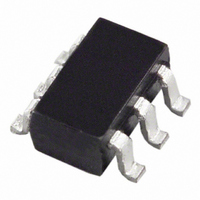
ADP3330ART-2.5-RL7 Analog Devices Inc, ADP3330ART-2.5-RL7 Datasheet - Page 7

ADP3330ART-2.5-RL7
Manufacturer Part Number
ADP3330ART-2.5-RL7
Description
IC REG LDO 200MA 2.5V SOT-23-6
Manufacturer
Analog Devices Inc
Series
anyCAP®r
Datasheet
1.ADP3330ARTZ3.3-RL7.pdf
(12 pages)
Specifications of ADP3330ART-2.5-RL7
Rohs Status
RoHS non-compliant
Design Resources
Half-Duplex, Isolated RS-485 Interface (CN0031)
Regulator Topology
Positive Fixed
Voltage - Output
2.5V
Voltage - Input
2.9 ~ 12 V
Voltage - Dropout (typical)
0.14V @ 200mA
Number Of Regulators
1
Current - Output
200mA
Operating Temperature
-40°C ~ 85°C
Mounting Type
Surface Mount
Package / Case
SOT-23-6
Current - Limit (min)
-
Other names
ADP3330ART-2.5RL7
Available stocks
Company
Part Number
Manufacturer
Quantity
Price
Company:
Part Number:
ADP3330ART-2.5-RL7
Manufacturer:
AD
Quantity:
118 000
Company:
Part Number:
ADP3330ART-2.5-RL7
Manufacturer:
microsemi
Quantity:
118 300
REV. A
THEORY OF OPERATION
The new anyCAP LDO ADP3330 uses a single control loop for
regulation and reference functions. The output voltage is sensed
by a resistive voltage divider consisting of R1 and R2 which is
varied to provide the available output voltage options. Feedback
is taken from this network by way of a series diode (D1) and a
second resistor divider (R3 and R4) to the input of an amplifier.
A very high gain error amplifier is used to control this loop.
The amplifier is constructed in such a way that at equilibrium it
produces a large, temperature-proportional input “offset voltage”
that is repeatable and very well controlled. The temperature-
proportional offset voltage is combined with the complementary
diode voltage to form a “virtual bandgap” voltage, implicit in
the network, although it never appears explicitly in the circuit.
Ultimately, this patented design makes it possible to control the
loop with only one amplifier. This technique also improves the
noise characteristics of the amplifier by providing more flexibil-
ity on the tradeoff of noise sources that leads to a low noise
design.
The R1, R2 divider is chosen in the same ratio as the bandgap
voltage to the output voltage. Although the R1, R2 resistor
divider is loaded by the diode D1, and a second divider consist-
ing of R3 and R4, the values are chosen to produce a tempera-
ture stable output. This unique arrangement specifically
corrects for the loading of the divider so that the error resulting
from base current loading in conventional circuits is avoided.
INPUT
NONINVERTING
WIDEBAND
DRIVER
Q1
Figure 20. Functional Block Diagram
ADP3330
COMPENSATION
CAPACITOR
g
m
PTAT
V
OS
R4
ATTENUATION
(V
GND
BANDGAP
CURRENT
R3
PTAT
/V
OUT
D1
OUTPUT
)
R2
R1
(a)
R
C
LOAD
LOAD
–7–
The patented amplifier controls a new and unique noninverting
driver that drives the pass transistor, Q1. The use of this special
noninverting driver enables the frequency compensation to
include the load capacitor in a pole splitting arrangement to
achieve reduced sensitivity to the value, type and ESR of the
load capacitance.
Most LDOs place strict requirements on the range of ESR
values for the output capacitor because they are difficult to
stabilize due to the uncertainty of load capacitance and resis-
tance. Moreover, the ESR value, required to keep conventional
LDOs stable, changes depending on load and temperature.
These ESR limitations make designing with LDOs more
difficult because of their unclear specifications and extreme
variations over temperature.
With the ADP3330 anyCAP LDO, this is no longer true. It
can be used with virtually any good quality capacitor, with no
constraint on the minimum ESR. The innovative design allows
the circuit to be stable with just a small 0.47 F capacitor on the
output. Additional advantages of the pole splitting scheme
include superior line noise rejection and very high regulator gain
which leads to excellent line and load regulation. An impressive
Additional features of the circuit include current limit, thermal
shutdown and noise reduction. Compared to standard solutions
that give warning after the output has lost regulation, the
ADP3330 provides improved system performance by enabling the
ERR pin to give warning just before the device loses regulation.
As the chip’s temperature rises above +165 C, the circuit
activates a soft thermal shutdown, indicated by a signal low on
the ERR pin, to reduce the current to a safe level.
1.4% accuracy is guaranteed over line, load and temperature.
ADP3330


