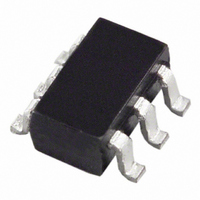
ADP3331ART-REEL Analog Devices Inc, ADP3331ART-REEL Datasheet - Page 3

ADP3331ART-REEL
Manufacturer Part Number
ADP3331ART-REEL
Description
IC REG LDO ADJ 200MA SOT-23-6
Manufacturer
Analog Devices Inc
Series
anyCAP®r
Datasheet
1.ADP3331ARTZ-REEL7.pdf
(12 pages)
Specifications of ADP3331ART-REEL
Rohs Status
RoHS non-compliant
Regulator Topology
Positive Adjustable
Voltage - Output
1.5 ~ 11.75 V
Voltage - Input
2.6 ~ 12 V
Voltage - Dropout (typical)
0.14V @ 200mA
Number Of Regulators
1
Current - Output
200mA
Operating Temperature
-40°C ~ 85°C
Mounting Type
Surface Mount
Package / Case
SOT-23-6
Current - Limit (min)
-
Available stocks
Company
Part Number
Manufacturer
Quantity
Price
Company:
Part Number:
ADP3331ART-REEL7
Manufacturer:
AD
Quantity:
155 170
Parameter
OUTPUT CURRENT IN
ERROR PIN OUTPUT LEAKAGE
ERROR PIN OUTPUT
NOTES
1
2
3
Specifications subject to change without notice.
ABSOLUTE MAXIMUM RATINGS*
Input Supply Voltage . . . . . . . . . . . . . . . . . . . . –0.3 V to +16 V
Shutdown Input Voltage . . . . . . . . . . . . . . . . . –0.3 V to +16 V
Power Dissipation . . . . . . . . . . . . . . . . . . . . Internally Limited
Operating Ambient Temperature Range . . . . –40∞C to +85∞C
Operating Junction Temperature Range . . . –40∞C to +125∞C
Storage Temperature Range . . . . . . . . . . . . –65∞C to +150∞C
Lead Temperature Range (Soldering 10 sec) . . . . . . . . . 300∞C
*Stresses above those listed under Absolute Maximum Ratings may cause perma-
Model
ADP3331ART
REV. A
CAUTION
ESD (electrostatic discharge) sensitive device. Electrostatic charges as high as 4000 V readily
accumulate on the human body and test equipment and can discharge without detection.
Although the ADP3331 features proprietary ESD protection circuitry, permanent damage may
occur on devices subjected to high energy electrostatic discharges. Therefore, proper ESD
precautions are recommended to avoid performance degradation or loss of functionality.
Ambient temperature of 85∞C corresponds to a junction temperature of 125∞C under typical full load test conditions.
Application stable with no load.
Assumes the use of ideal resistors. Overall accuracy also depends on the tolerance of the external resistors used to set the output voltage.
nent damage to the device. This is a stress rating only; functional operation of the
device at these or any other conditions above those listed in the operational
sections of this specification is not implied. Exposure to absolute maximum rating
conditions for extended periods may affect device reliability.
q
q
Vapor Phase (60 sec) . . . . . . . . . . . . . . . . . . . . . . . . . 215∞C
Infrared (15 sec) . . . . . . . . . . . . . . . . . . . . . . . . . . . . . 220∞C
SHUTDOWN MODE
LOW VOLTAGE
JA
JA
(4-Layer Board) . . . . . . . . . . . . . . . . . . . . . . . . 165∞C/W
(2-Layer Board) . . . . . . . . . . . . . . . . . . . . . . . . 190∞C/W
ADJ
Output
Voltage
ORDERING GUIDE
Package Option
RT-6 (SOT-23-6)
Symbol
I
I
V
OSD
EL
EOL
Branding
L9B
Conditions
T
T
V
I
SINK
EO
A
A
= 85∞C @ V
= 25∞C @ V
= 5 V
= 400 mA
–3–
Pin
1
2
3
4
5
6
IN
IN
= 12 V
= 12 V
Name
OUT
IN
ERR
GND
FB
SD
PIN FUNCTION DESCRIPTIONS
PIN CONFIGURATION
OUT
ERR
Function
Output of the Regulator. Bypass to ground
with a 0.47 mF or larger capacitor.
Regulator Input.
Open Collector Output that goes low to
indicate that the output is about to go out
of regulation.
Ground.
Feedback Input. Connect to an external
resistor divider, which sets the output
voltage.
Active Low Shutdown Pin. Connect to
ground to disable the regulator output.
When shutdown is not used, this pin
should be connected to the input pin.
IN
1
2
3
(Not to Scale)
ADP3331
TOP VIEW
Min
WARNING!
6
5
4
Typ
0.19
SD
FB
GND
ESD SENSITIVE DEVICE
Max
1
2
1
0.40
ADP3331
Unit
mA
mA
mA
V


