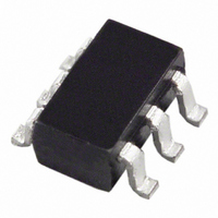
ADP3331ART-REEL Analog Devices Inc, ADP3331ART-REEL Datasheet - Page 8

ADP3331ART-REEL
Manufacturer Part Number
ADP3331ART-REEL
Description
IC REG LDO ADJ 200MA SOT-23-6
Manufacturer
Analog Devices Inc
Series
anyCAP®r
Datasheet
1.ADP3331ARTZ-REEL7.pdf
(12 pages)
Specifications of ADP3331ART-REEL
Rohs Status
RoHS non-compliant
Regulator Topology
Positive Adjustable
Voltage - Output
1.5 ~ 11.75 V
Voltage - Input
2.6 ~ 12 V
Voltage - Dropout (typical)
0.14V @ 200mA
Number Of Regulators
1
Current - Output
200mA
Operating Temperature
-40°C ~ 85°C
Mounting Type
Surface Mount
Package / Case
SOT-23-6
Current - Limit (min)
-
Available stocks
Company
Part Number
Manufacturer
Quantity
Price
Company:
Part Number:
ADP3331ART-REEL7
Manufacturer:
AD
Quantity:
155 170
ADP3331
Calculating Junction Temperature
Device power dissipation is calculated as follows:
Where I
V
Assuming that the worst case operating conditions are I
200 mA, I
device power dissipation is
The proprietary package used on the ADP3331 has a thermal
resistance of 165∞C/W when placed on a 4-layer board and
190∞C/W when placed on a 2-layer board. This allows the ambient
temperature to be significantly higher for a given power dissipa-
tion than with a standard package. Assuming a 4-layer board, the
junction temperature rise above ambient will be approximately
equal to
To limit the junction temperature to 125∞C, the maximum
allowable ambient temperature is
Shutdown Mode
Applying a TTL level high signal to the shutdown (SD) pin, or
tying it to the input pin, will turn the output ON. Pulling the
SD to 0.4 V or below, or tying it to ground, will turn the output
OFF. In shutdown mode, the quiescent current is reduced to
less than 1 mA.
Error Flag Dropout Detector
The ADP3331 will maintain its output voltage over a wide
range of load, input voltage, and temperature conditions. If the
output is about to lose regulation due to the input voltage
approaching the dropout level, the error flag will be activated.
The ERR output is an open collector, which will be driven low.
Once set, the ERR flag’s hysteresis will keep the output low until
a small margin of operating range is restored either by raising
the supply voltage or reducing the load.
Low Voltage Applications
In applications where the output voltage is 2.2 V or less, the
ADP3331 may begin to exhibit some turn-on overshoot. The
SILICON
IN
T
P
P
D T
D
and V
D
A MAX
DIE
(
=
=
J
A
LOAD
NORMAL SOT-23-6 PACKAGE
(
(
V
4 2
=
OUT
GND
.
)
IN
0 257
= +
.
V
and I
-
are the input and output voltages, respectively.
= 4 mA, V
Figure 4. Chip-on-Lead Package
V
-
125
OUT
W
3 0
GND
.
o
C
)
¥
V
I
165
LOAD
-
are load current and ground current and
)
200
42 4
IN
o
C W
.
= 4.2 V, and V
+
/
mA
o
C
( )
V
ELECTRICALLY
IN
=
=
SILICON DIE
DIE ATTACH
+
82 6
42 4
ISOLATED
(
I
4 2
GND
.
.
.
WITH
o
o
V
C
C
)
OUT
4
THERMALLY ENHANCED
CHIP-ON-LEAD PACKAGE
mA
= 3.0 V, the
=
257
LOAD
mW
(10)
(11)
=
(8)
(9)
–8–
degree of overshoot is determined by several factors: the output
voltage setting, the output load, the noise reduction capacitor,
and the output capacitor.
The output voltage setting is determined by the application and
cannot be tailored for minimum overshoot. In general, for output
voltages of 2.2 V or less, the overshoot becomes larger as the
output voltage decreases.
The output load is also determined by the system requirements.
However, if the ADP3331 has no load on the output during
startup, a small amount of preload can be added to minimize
overshoot. A preload of 2 mA to 20 mA is recommended.
A noise reduction capacitor, if not already being used, is sug-
gested to reduce the overshoot. Values in the range of 10 pF to
100 pF work best, along with the preload suggested previously.
The output capacitor can be adjusted to minimize the over-
shoot. Values in the 0.47 mF to 1.0 mF range should be used in
conjunction with the preload and noise reduction capacitor.
Further increases in the output capacitance may be acceptable if
the output already has a sizable load during startup.
Higher Output Current
The ADP3331 can source up to 200 mA without any heat sink
or pass transistor. If higher current is needed, an appropriate pass
transistor can be used, as in Figure 5, to increase the output
current to 1 A.
Printed Circuit Board Layout Considerations
Use the following general guidelines when designing printed
circuit boards:
1. PC board traces with larger cross sectional areas will remove
2. The thermal resistance can be decreased by approximately
3. The feedback pin is a high impedance input, and care should
*REQUIRES HEAT SINK
more heat from the ADP3331. For optimum heat transfer,
specify thick copper and use wide traces.
10% by adding a few square centimeters of copper area to
the lands connected to the pins of the LDO.
be taken when making a connection to this pin. The voltage
setting resistors and noise reduction network must be located
as close as possible. Long PC board traces are not recom-
mended. Avoid routing traces near possible noise sources.
V
IN
= 3.3V
Figure 5. High Output Current Linear Regulator
47 F
C1
50
SD
R1
ADP3331
MJE253*
GND
IN
ERR
OUT
FB
C2
10 F
340k
698k
V
OUT
= 1.8V @ 1A
REV. A


