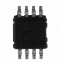
LP2966IMM-2830/NOPB National Semiconductor, LP2966IMM-2830/NOPB Datasheet

LP2966IMM-2830/NOPB
Specifications of LP2966IMM-2830/NOPB
LP2966IMM-2830TR
Related parts for LP2966IMM-2830/NOPB
LP2966IMM-2830/NOPB Summary of contents
Page 1
... ERROR2 are open drain outputs. These pins must be connected to ground if not used. # Minimum output capacitance is 1µF to insure stability over full load current range. More capacitance improves superior dynamic performance and provides additional stability margin. © 2005 National Semiconductor Corporation Features n Ultra low drop-out voltage n Low ground pin current < ...
Page 2
Block Diagram Connection Diagram www.national.com 10085032 Top View Mini SO-8 Package 8-Lead Small Outline Integrated Circuit (SOIC) Package Code: MSOP-8 2 10085031 ...
Page 3
... LP2966IMMX-3325 LARB LP2966IMM-3030 LACB LP2966IMMX-3030 LACB LP2966IMM-2830 LASB LP2966IMMX-2830 LASB LP2966IMM-2828 LABB LP2966IMMX-2828 LABB LP2966IMM-2525 LAAB LP2966IMMX-2525 LAAB LP2966IMM-2518 LJKB LP2966IMMX-2518 LJKB LP2966IMM-1833 LCFB LP2966IMMX-1833 LCFB LP2966IMM-1830 LEYB LP2966IMMX-1830 LEYB LP2966IMM-1828 LAVB LP2966IMMX-1828 LAVB LP2966IMM-1818 LA9B LP2966IMMX-1818 LA9B 3 Supplied As: 1000 units on tape and reel ...
Page 4
... OUT OUT(NOM) (Note 2), (Note 14) 4 −0.3V to (Vin + 0.3V) (Note 1) 2.7V to 7.0V −0.3V to (Vin + 0.3V) −40˚C to +125˚C = 1mA 1µ OUT IN SD1 SD2 LP2966IMM (Note 5) 4) Min Max 0.0 − 0.0 −1.5 1.5 -3.5 3.5 0.1 0.1 0.0004 0.9 2.0 3 ...
Page 5
... V + 0.3V OUT 120Hz 3.3V OUT f =120Hz BW = 10Hz − 100kHz 10µF OUT BW = 300Hz − 300kHz 10µF OUT and V terminals that is normally reverse-biased. Reversing the polarity from V IN OUT 5 = 1mA 1µ OUT IN SD1 SD2 LP2966IMM (Note 5) 4) Min Max 0.015 0 ...
Page 6
Electrical Characteristics Note 13: Output voltage tolerance specification also includes the line regulation and load regulation. Note 14: LP2966 has fold back current limited short circuit protection. The knee is the current at which the output voltage drops 10% below ...
Page 7
Typical Performance Characteristics C =1µ 1mA, C =1µF, V OUT OUT IN SD1 Ground Pin Current vs Supply Voltage (one LDO on) Ground Pin Current vs Load Current over temperature (one LDO on) Output Voltage vs Temperature Unless ...
Page 8
Typical Performance Characteristics C =1µ 1mA, C =1µF, V OUT OUT IN Input Voltage vs Output Voltage Ground Pin Current vs Input Voltage (Both LDOs off) Line Transient Response (C = 2.2µF, I OUT OUT www.national.com Unless otherwise ...
Page 9
Typical Performance Characteristics C =1µ 1mA, C =1µF, V OUT OUT IN SD1 Line Transient Response (C = 2.2µ 100mA) OUT OUT Line Transient Response (C = 10µ 1mA) OUT OUT Line Transient Response ...
Page 10
Typical Performance Characteristics C =1µ 1mA, C =1µF, V OUT OUT IN Load Transient Response (C Load Transient Response (C Cross-Channel Isolation vs Frequency (I =1mA, I OUT1 OUT2 www.national.com Unless otherwise specified ...
Page 11
Typical Performance Characteristics C =1µ 1mA, C =1µF, V OUT OUT IN SD1 Output Voltage Cross-Coupling Power Supply Ripple Rejection Unless otherwise specified and T = 25˚C. (Continued) SD2 IN A 10085013 ...
Page 12
Applications Information Input Capacitor Selection LP2966 requires a minimum input capacitance of 1µF be- tween the input and ground pins to prevent any impedance interactions with the supply. This capacitor should be located very close to the input pin. This ...
Page 13
Applications Information The internal error flag comparators have open drain output stages. Hence, the ERROR pins should be pulled high through a pull up resistor. Although the ERROR pin can sink current of 1mA, this current adds to the battery ...
Page 14
Applications Information FIGURE 4. FIGURE 5. FIGURE 6. www.national.com (Continued) 10085036 10085037 10085038 14 10085039 FIGURE 7. 10085040 FIGURE 8. ...
Page 15
... BANNED SUBSTANCE COMPLIANCE National Semiconductor manufactures products and uses packing materials that meet the provisions of the Customer Products Stewardship Specification (CSP-9-111C2) and the Banned Substances and Materials of Interest Specification (CSP-9-111S2) and contain no ‘‘Banned Substances’’ as defined in CSP-9-111S2. ...


