SP721AB Littelfuse Inc, SP721AB Datasheet

TVS ARRAY ESD 6 INPUT 8-SOIC

SP721AB

Manufacturer Part Number
SP721AB
Description
TVS ARRAY ESD 6 INPUT 8-SOIC
Manufacturer
Littelfuse Inc
Series
SP721r
Datasheet

Specifications of SP721AB

Package / Case
8-SOIC (3.9mm Width)
Voltage - Working
30V
Technology
Mixed Technology
Number Of Circuits
6
Applications
General Purpose
Current Rating
+/- 5 A
Forward Voltage Drop
2 V
Operating Voltage
2 V to 30 V
Channels
6 Channels
Capacitance
3 pF
Operating Temperature Range
- 40 C to + 105 C
Lead Free Status / RoHS Status
Contains lead / RoHS non-compliant
Power (watts)
-
Voltage - Clamping
-
Lead Free Status / RoHS Status
Lead free / RoHS Compliant, Contains lead / RoHS non-compliant
Other names
F2165

Available stocks

Company
Part Number
Manufacturer
Quantity
Price
Part Number:
SP721AB
Manufacturer:
N/A
Quantity:
20 000
Part Number:
SP721ABG
Manufacturer:
LITTEFUSE
Quantity:
20 000
Part Number:
SP721ABT
Manufacturer:
INTERSIL
Quantity:
20 000
Company:
Part Number:
SP721ABT
Quantity:
2 264
Part Number:
SP721ABTG
Manufacturer:
NEC
Quantity:
6 221
Part Number:
SP721ABTG
Manufacturer:
LITTEFUSE
Quantity:
20 000
TVS Diode Arrays
Electronic Protection Array for ESD and Overvoltage Protection
SP721
The SP721 is an array of SCR/Diode bipolar structures for ESD and
over-voltage protection to sensitive input circuits. The SP721 has 2
protection SCR/Diode device structures per input. There are a total of
6 available inputs that can be used to protect up to 6 external signal or
bus lines. Over-voltage protection is from the IN (Pins 1 - 3 and Pins
5 - 7) to V+ or V-.
The SCR structures are designed for fast triggering at a threshold of one
+V BE diode threshold above V+ (Pin 8) or a -V BE diode threshold below
V- (Pin 4). From an IN input, a clamp to V+ is activated if a transient
pulse causes the input to be increased to a voltage level greater than
one V BE above V+. A similar clamp to V- is activated if a negative pulse,
one V BE less than V-, is applied to an IN input. Standard ESD Human
Body Model (HBM) Capability is:
Pinout
Refer to Figure 1 and Table 1 for further detail. Refer to Application
Notes AN9304 and AN9612 for additional information.
Ordering Information
SP721AP
SP721AB
SP721ABT
IEC 61000-4-2
MIL-STD-3015.7 Direct, In-Circuit
234
PART NO.
STANDARD
HBM
TEMP. RANGE
IN
IN
IN
V-
-40 to 105
-40 to 105
-40 to 105
Air
Direct
Direct, Dual Pins
SP721 (PDIP, SOIC)
(
o
1
2
3
4
C)
MODE
TOP VIEW
8 Ld PDIP
8 Ld SOIC
8 Ld SOIC
Tape and Reel
PACKAGE
1.5kΩ
330Ω
330Ω
330Ω
R
8
7
6
5
V+
IN
IN
IN
150pF
150pF
150pF
100pF
C
M8.15
E8.3
M8.15
PKG.
NO.
ESD (V)
>15kV
>15kV
>4kV
>8kV
w w w . l i t t e l f u s e . c o m
Order
2000
1960
2500
Min.
Features
• ESD Interface Capability for HBM Standards
• High Peak Current Capability
• Designed to Provide Over-Voltage Protection
• Fast Switching . . . . . . . . . . . . . . . . . . . . . . . . . . . . . . . . . 2ns Rise Time
• Low Input Leakages . . . . . . . . . . . . . . . . . . . . . . . . 1nA at 25
• Low Input Capacitance . . . . . . . . . . . . . . . . . . . . . . . . . . . . . 3pF Typical
• An Array of 6 SCR/Diode Pairs
• Operating Temperature Range . . . . . . . . . . . . . . . . . . . . -40
Applications
• Microprocessor/Logic Input Protection
• Data Bus Protection
• Analog Device Input Protection
• Voltage Clamp
Functional Block Diagram
- MIL STD 3015.7 . . . . . . . . . . . . . . . . . . . . . . . . . . . . . . . . . . . . 15kV
- IEC 61000-4-2, Direct Discharge,
- Single Input. . . . . . . . . . . . . . . . . . . . . . . . . . . . . . . . . . 4kV (Level 2)
- Two Inputs in Parallel . . . . . . . . . . . . . . . . . . . . . . . . . . 8kV (Level 4)
- IEC 61000-4-2, Air Discharge . . . . . . . . . . . . . . . . . . 15kV (Level 4)
- IEC 61000-4-5 (8/20µs). . . . . . . . . . . . . . . . . . . . . . . . . . . . . . . . ±3A
- Single Pulse, 100µs Pulse Width . . . . . . . . . . . . . . . . . . . . . . . . ±2A
- Single Pulse, 4µs Pulse Width . . . . . . . . . . . . . . . . . . . . . . . . . . ±5A
- Single-Ended Voltage Range to . . . . . . . . . . . . . . . . . . . . . . . . +30V
- Differential Voltage Range to. . . . . . . . . . . . . . . . . . . . . . . . . . . ±15V
V+
IN
V-
8
1
4
IN
2
IN
3, 5-7
o
C to 105
o
C Typical
o
C

Related parts for SP721AB

SP721AB Summary of contents

Page 1

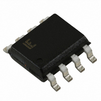
... Refer to Figure 1 and Table 1 for further detail. Refer to Application Notes AN9304 and AN9612 for additional information. Ordering Information TEMP. RANGE o PART NO PACKAGE SP721AP -40 to 105 8 Ld PDIP SP721AB -40 to 105 8 Ld SOIC SP721ABT -40 to 105 8 Ld SOIC Tape and Reel Pinout SP721 (PDIP, SOIC) TOP VIEW ...

Page 2

TVS Diode Arrays Electronic Protection Array for ESD and Overvoltage Protection SP721 Absolute Maximum Ratings Continuous Supply Voltage, (V+) - (V-). . . . . . . . . . . . . . . . . . . . ...

Page 3

TVS Diode Arrays Electronic Protection Array for ESD and Overvoltage Protection SP721 100 SINGLE PULSE 600 800 FORWARD SCR VOLTAGE DROP (mV) FIGURE 2. LOW CURRENT SCR FORWARD VOLTAGE ...

Page 4

TVS Diode Arrays Electronic Protection Array for ESD and Overvoltage Protection SP721 Peak Transient Current Capability of the SP721 The peak transient current capability rises sharply as the width of the current pulse narrows. Destructive testing was done to fully ...

Page 5

TVS Diode Arrays Electronic Protection Array for ESD and Overvoltage Protection SP721 Dual-In-Line Plastic Packages (PDIP INDEX N/2 AREA -B- -A- D BASE PLANE -C- SEATING PLANE 0.010 ...

Page 6

TVS Diode Arrays Electronic Protection Array for ESD and Overvoltage Protection SP721 Small Outline Plastic Packages (SOIC) N INDEX 0.25(0.010) H AREA E - SEATING PLANE - -C- µ 0.10(0.004) 0.25(0.010) M ...

Related keywords