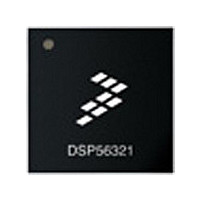
DSP56303VL100 Freescale Semiconductor, DSP56303VL100 Datasheet - Page 19

DSP56303VL100
Manufacturer Part Number
DSP56303VL100
Description
IC DSP 24BIT 100MHZ 196-MAPBGA
Manufacturer
Freescale Semiconductor
Series
DSP563xxr
Type
Fixed Pointr
Datasheet
1.DSP56303AG100.pdf
(108 pages)
Specifications of DSP56303VL100
Interface
Host Interface, SSI, SCI
Clock Rate
100MHz
Non-volatile Memory
ROM (576 B)
On-chip Ram
24kB
Voltage - I/o
3.30V
Voltage - Core
3.30V
Operating Temperature
-40°C ~ 100°C
Mounting Type
Surface Mount
Package / Case
196-MAPBGA
Device Core Size
24b
Format
Fixed Point
Clock Freq (max)
100MHz
Mips
100
Device Input Clock Speed
100MHz
Ram Size
24KB
Program Memory Size
Not RequiredKB
Operating Supply Voltage (typ)
3.3V
Operating Supply Voltage (min)
3V
Operating Supply Voltage (max)
3.6V
Operating Temp Range
-40C to 100C
Operating Temperature Classification
Industrial
Mounting
Surface Mount
Pin Count
196
Package Type
MA-BGA
Package
196MA-BGA
Maximum Speed
100 MHz
Device Million Instructions Per Second
100 MIPS
Lead Free Status / RoHS Status
Lead free / RoHS Compliant
Available stocks
Company
Part Number
Manufacturer
Quantity
Price
Company:
Part Number:
DSP56303VL100
Manufacturer:
FUJI
Quantity:
1 000
Company:
Part Number:
DSP56303VL100
Manufacturer:
FREESCALE
Quantity:
672
Company:
Part Number:
DSP56303VL100
Manufacturer:
Freescale Semiconductor
Quantity:
10 000
Company:
Part Number:
DSP56303VL100B1
Manufacturer:
Freescale Semiconductor
Quantity:
10 000
1.11 Timers
The DSP56303 has three identical and independent timers. Each timer can use internal or external clocking and can
either interrupt the DSP56303 after a specified number of events (clocks) or signal an external device after
counting a specific number of internal events.
Freescale Semiconductor
TIO0
TIO1
TIO2
Notes:
Signal Name
1.
2.
3.
In the Stop state, the signal maintains the last state as follows:
• If the last state is input, the signal is an ignored input.
• If the last state is output, the signal is tri-stated.
The Wait processing state does not affect the signal state.
All inputs are 5 V tolerant.
Input or Output
Input or Output
Input or Output
Type
Ignored Input
Ignored Input
Ignored Input
State During
Reset
Table 1-15.
DSP56303 Technical Data, Rev. 11
1,2
Timer 0 Schmitt-Trigger Input/Output— When Timer 0 functions as an
external event counter or in measurement mode, TIO0 is used as input. When
Timer 0 functions in watchdog, timer, or pulse modulation mode, TIO0 is used
as output.
The default mode after reset is GPIO input. TIO0 can be changed to output or
configured as a timer I/O through the Timer 0 Control/Status Register (TCSR0).
Timer 1 Schmitt-Trigger Input/Output— When Timer 1 functions as an
external event counter or in measurement mode, TIO1 is used as input. When
Timer 1 functions in watchdog, timer, or pulse modulation mode, TIO1 is used
as output.
The default mode after reset is GPIO input. TIO1 can be changed to output or
configured as a timer I/O through the Timer 1 Control/Status Register (TCSR1).
Timer 2 Schmitt-Trigger Input/Output— When Timer 2 functions as an
external event counter or in measurement mode, TIO2 is used as input. When
Timer 2 functions in watchdog, timer, or pulse modulation mode, TIO2 is used
as output.
The default mode after reset is GPIO input. TIO2 can be changed to output or
configured as a timer I/O through the Timer 2 Control/Status Register (TCSR2).
Triple Timer Signals
Signal Description
Timers
1-15


