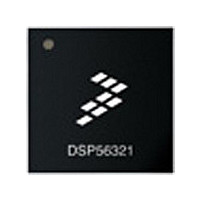
DSP56303VL100 Freescale Semiconductor, DSP56303VL100 Datasheet - Page 32

DSP56303VL100
Manufacturer Part Number
DSP56303VL100
Description
IC DSP 24BIT 100MHZ 196-MAPBGA
Manufacturer
Freescale Semiconductor
Series
DSP563xxr
Type
Fixed Pointr
Datasheet
1.DSP56303AG100.pdf
(108 pages)
Specifications of DSP56303VL100
Interface
Host Interface, SSI, SCI
Clock Rate
100MHz
Non-volatile Memory
ROM (576 B)
On-chip Ram
24kB
Voltage - I/o
3.30V
Voltage - Core
3.30V
Operating Temperature
-40°C ~ 100°C
Mounting Type
Surface Mount
Package / Case
196-MAPBGA
Device Core Size
24b
Format
Fixed Point
Clock Freq (max)
100MHz
Mips
100
Device Input Clock Speed
100MHz
Ram Size
24KB
Program Memory Size
Not RequiredKB
Operating Supply Voltage (typ)
3.3V
Operating Supply Voltage (min)
3V
Operating Supply Voltage (max)
3.6V
Operating Temp Range
-40C to 100C
Operating Temperature Classification
Industrial
Mounting
Surface Mount
Pin Count
196
Package Type
MA-BGA
Package
196MA-BGA
Maximum Speed
100 MHz
Device Million Instructions Per Second
100 MIPS
Lead Free Status / RoHS Status
Lead free / RoHS Compliant
Available stocks
Company
Part Number
Manufacturer
Quantity
Price
Company:
Part Number:
DSP56303VL100
Manufacturer:
FUJI
Quantity:
1 000
Company:
Part Number:
DSP56303VL100
Manufacturer:
FREESCALE
Quantity:
672
Company:
Part Number:
DSP56303VL100
Manufacturer:
Freescale Semiconductor
Quantity:
10 000
Company:
Part Number:
DSP56303VL100B1
Manufacturer:
Freescale Semiconductor
Quantity:
10 000
Specifications
2.5.5
2.5.5.1 SRAM Timing
2-12
No.
100
101
102
103
104
105
106
107
108
109
110
Address valid and AA assertion pulse width
Address and AA valid to WR assertion
WR assertion pulse width
WR deassertion to address not valid
Address and AA valid to input data valid
RD assertion to input data valid
RD deassertion to data not valid (data hold time)
Address valid to WR deassertion
Data valid to WR deassertion (data setup time)
Data hold time from WR deassertion
WR assertion to data active
External Memory Expansion Port (Port A)
Characteristics
2
Table 2-8.
DSP56303 Technical Data, Rev. 11
2
SRAM Read and Write Accesses
Symbol
t
t
DS
t
RC
AA
t
t
t
t
t
t
OHZ
t
WP
WR
AW
—
OE
DH
, t
AS
, t
(t
DW
WC
AC
)
(WS + 0.25) × T
(WS + 0.75) × T
(WS + 0.75) × T
(WS − 0.25) × T
(WS − 0.5) × T
(WS + 1) × T
(WS + 2) × T
(WS + 3) × T
–0.25 × T
0.25 × T
0.25 × T
0.75 × T
1.25 × T
0.25 × T
1.25 × T
2.25 × T
0.25 × T
1.25 × T
2.25 × T
0.75 × T
Expression
WS × T
1.5 × T
[1 ≤ WS ≤ 3]
[4 ≤ WS ≤ 7]
[2 ≤ WS ≤ 3]
[2 ≤ WS ≤ 3]
[1 ≤ WS ≤ 3]
[4 ≤ WS ≤ 7]
[1 ≤ WS ≤ 3]
[4 ≤ WS ≤ 7]
[2 ≤ WS ≤ 3]
[WS ≥ 8]
[WS = 1]
[WS ≥ 4]
[WS = 1]
[WS ≥ 4]
[WS ≥ 8]
[WS ≥ 1]
[WS ≥ 1]
[WS ≥ 1]
[WS ≥ 1]
[WS ≥ 8]
[WS = 1]
[WS ≥ 4]
C
C
C
C
C
C
C
C
C
C
C
C
C
C
− 4.0
− 4.0
– 3.7
− 2.0
− 2.0
− 2.0
− 2.0
− 4.0
− 4.0
− 2.0
− 2.0
− 2.0
− 3.7
C
C
C
− 3.7
C
C
C
C
C
− 4.0
− 4.0
− 4.0
− 4.0
1
− 3.0
– 5.0
− 5.0
− 4.0
Freescale Semiconductor
106.0
Min
16.0
56.0
10.5
11.0
16.0
31.0
18.5
13.5
10.5
20.5
–1.2
–6.2
0.5
5.5
0.5
8.5
0.0
4.5
0.5
3.8
—
—
100 MHz
Max
12.5
7.5
—
—
—
—
—
—
—
—
—
—
—
—
—
—
—
—
—
—
—
—
—
Unit
ns
ns
ns
ns
ns
ns
ns
ns
ns
ns
ns
ns
ns
ns
ns
ns
ns
ns
ns
ns
ns
ns
ns


