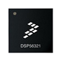
DSP56303VL100 Freescale Semiconductor, DSP56303VL100 Datasheet - Page 44

DSP56303VL100
Manufacturer Part Number
DSP56303VL100
Description
IC DSP 24BIT 100MHZ 196-MAPBGA
Manufacturer
Freescale Semiconductor
Series
DSP563xxr
Type
Fixed Pointr
Datasheet
1.DSP56303AG100.pdf
(108 pages)
Specifications of DSP56303VL100
Interface
Host Interface, SSI, SCI
Clock Rate
100MHz
Non-volatile Memory
ROM (576 B)
On-chip Ram
24kB
Voltage - I/o
3.30V
Voltage - Core
3.30V
Operating Temperature
-40°C ~ 100°C
Mounting Type
Surface Mount
Package / Case
196-MAPBGA
Device Core Size
24b
Format
Fixed Point
Clock Freq (max)
100MHz
Mips
100
Device Input Clock Speed
100MHz
Ram Size
24KB
Program Memory Size
Not RequiredKB
Operating Supply Voltage (typ)
3.3V
Operating Supply Voltage (min)
3V
Operating Supply Voltage (max)
3.6V
Operating Temp Range
-40C to 100C
Operating Temperature Classification
Industrial
Mounting
Surface Mount
Pin Count
196
Package Type
MA-BGA
Package
196MA-BGA
Maximum Speed
100 MHz
Device Million Instructions Per Second
100 MIPS
Lead Free Status / RoHS Status
Lead free / RoHS Compliant
Available stocks
Company
Part Number
Manufacturer
Quantity
Price
Company:
Part Number:
DSP56303VL100
Manufacturer:
FUJI
Quantity:
1 000
Company:
Part Number:
DSP56303VL100
Manufacturer:
FREESCALE
Quantity:
672
Company:
Part Number:
DSP56303VL100
Manufacturer:
Freescale Semiconductor
Quantity:
10 000
Company:
Part Number:
DSP56303VL100B1
Manufacturer:
Freescale Semiconductor
Quantity:
10 000
Specifications
2.5.5.3 Synchronous Timings
2-24
Notes:
No.
198
199
200
201
202
203
204
205
206
207
208
209
210
211
CLKOUT high to address, and AA valid
CLKOUT high to address, and AA invalid
TA valid to CLKOUT high (set-up time)
CLKOUT high to TA invalid (hold time)
CLKOUT high to data out active
CLKOUT high to data out valid
CLKOUT high to data out invalid
CLKOUT high to data out high impedance
Data in valid to CLKOUT high (set-up)
CLKOUT high to data in invalid (hold)
CLKOUT high to RD assertion
CLKOUT high to RD deassertion
CLKOUT high to WR assertion
CLKOUT high to WR deassertion
1.
2.
3.
4.
5.
6.
Use external bus synchronous timings only for reference to the clock and not for relative timings.
Synchronous Bus Arbitration is not recommended. Use Asynchronous mode whenever possible.
WS is the number of wait states specified in the BCR.
If WS > 1, WR assertion refers to the next rising edge of CLKOUT.
Use the expression to compute the maximum or minimum value listed, as appropriate. For timing 210, the minimum is an
absolute value.
T198 and T199 are valid for Address Trace mode if the ATE bit in the Operating Mode Register is set. when this mode is
enabled, use the status of BR (See T212) to determine whether the access referenced by A[0–17] is internal or external.
Characteristics
Table 2-13.
2
DSP56303 Technical Data, Rev. 11
6
6
External Bus Synchronous Timings
maximum: 0.75 × T
maximum: 0.5 × T
for WS = 1 or WS ≥ 4
Expression
0.25 × T
0.25 × T
for 2 ≤ WS ≤ 3
0.25 × T
0.25 × T
0.25 × T
0.25 × T
C
C
+ 4.0
+ 4.0
C
C
C
C
3,4,5
C
C
+ 4.3
+ 2.5
1,2
Min
2.5
4.0
0.0
2.5
2.5
4.0
0.0
6.7
0.0
5.0
0.0
0.0
Freescale Semiconductor
—
—
—
100 MHz
Max
10.0
6.5
6.5
2.5
4.0
9.3
4.3
3.8
—
—
—
—
—
—
—
Unit
ns
ns
ns
ns
ns
ns
ns
ns
ns
ns
ns
ns
ns
ns
ns


