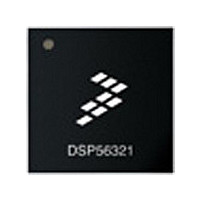
DSP56303VL100 Freescale Semiconductor, DSP56303VL100 Datasheet - Page 7

DSP56303VL100
Manufacturer Part Number
DSP56303VL100
Description
IC DSP 24BIT 100MHZ 196-MAPBGA
Manufacturer
Freescale Semiconductor
Series
DSP563xxr
Type
Fixed Pointr
Datasheet
1.DSP56303AG100.pdf
(108 pages)
Specifications of DSP56303VL100
Interface
Host Interface, SSI, SCI
Clock Rate
100MHz
Non-volatile Memory
ROM (576 B)
On-chip Ram
24kB
Voltage - I/o
3.30V
Voltage - Core
3.30V
Operating Temperature
-40°C ~ 100°C
Mounting Type
Surface Mount
Package / Case
196-MAPBGA
Device Core Size
24b
Format
Fixed Point
Clock Freq (max)
100MHz
Mips
100
Device Input Clock Speed
100MHz
Ram Size
24KB
Program Memory Size
Not RequiredKB
Operating Supply Voltage (typ)
3.3V
Operating Supply Voltage (min)
3V
Operating Supply Voltage (max)
3.6V
Operating Temp Range
-40C to 100C
Operating Temperature Classification
Industrial
Mounting
Surface Mount
Pin Count
196
Package Type
MA-BGA
Package
196MA-BGA
Maximum Speed
100 MHz
Device Million Instructions Per Second
100 MIPS
Lead Free Status / RoHS Status
Lead free / RoHS Compliant
Available stocks
Company
Part Number
Manufacturer
Quantity
Price
Company:
Part Number:
DSP56303VL100
Manufacturer:
FUJI
Quantity:
1 000
Company:
Part Number:
DSP56303VL100
Manufacturer:
FREESCALE
Quantity:
672
Company:
Part Number:
DSP56303VL100
Manufacturer:
Freescale Semiconductor
Quantity:
10 000
Company:
Part Number:
DSP56303VL100B1
Manufacturer:
Freescale Semiconductor
Quantity:
10 000
1.1 Power
1.2 Ground
Freescale Semiconductor
V
V
V
V
V
V
V
Note: The user must provide adequate external decoupling capacitors for all power connections.
Ground Name
GND
GND
GND
GND
GND
GND
GND
GND
GND
Notes:
Power Name
CCP
CCQ
CCA
CCD
CCC
CCH
CCS
P
P1
Q
A
D
C
H
S
3
2
2
2
2
2
2
1.
2.
3.
The user must provide adequate external decoupling capacitors for all GND connections.
These connections are only used on the TQFP package.
These connections are common grounds used on the MAP-BGA package.
PLL Power—V
an extremely low impedance path to the V
Quiet Power—An isolated power for the core processing logic. This input must be isolated externally from all other chip
power inputs.
Address Bus Power—An isolated power for sections of the address bus I/O drivers. This input must be tied externally
to all other chip power inputs, except V
Data Bus Power—An isolated power for sections of the data bus I/O drivers. This input must be tied externally to all
other chip power inputs, except V
Bus Control Power—An isolated power for the bus control I/O drivers. This input must be tied externally to all other
chip power inputs, except V
Host Power—An isolated power for the HI08 I/O drivers. This input must be tied externally to all other chip power
inputs, except V
ESSI, SCI, and Timer Power—An isolated power for the ESSI, SCI, and timer I/O drivers. This input must be tied
externally to all other chip power inputs, except V
PLL Ground—Ground-dedicated for PLL use. The connection should be provided with an extremely low-impedance
path to ground. V
package.
PLL Ground 1—Ground-dedicated for PLL use. The connection should be provided with an extremely low-impedance
path to ground.
Quiet Ground—An isolated ground for the internal processing logic. This connection must be tied externally to all other
chip ground connections, except GND
Address Bus Ground—An isolated ground for sections of the address bus I/O drivers. This connection must be tied
externally to all other chip ground connections, except GND
decoupling capacitors.
Data Bus Ground—An isolated ground for sections of the data bus I/O drivers. This connection must be tied externally
to all other chip ground connections, except GND
capacitors.
Bus Control Ground—An isolated ground for the bus control I/O drivers. This connection must be tied externally to all
other chip ground connections, except GND
capacitors.
Host Ground—An isolated ground for the HI08 I/O drivers. This connection must be tied externally to all other chip
ground connections, except GND
ESSI, SCI, and Timer Ground—An isolated ground for the ESSI, SCI, and timer I/O drivers. This connection must be
tied externally to all other chip ground connections, except GND
decoupling capacitors.
Ground—Connected to an internal device ground plane.
CC
CCQ
CCP
dedicated for PLL use. The voltage should be well-regulated and the input should be provided with
.
should be bypassed to GND
CCQ
DSP56303 Technical Data, Rev. 11
.
Table 1-2.
P
CCQ
Table 1-3.
and GND
.
P
CCQ
and GND
CC
.
P
P1
power rail.
and GND
. The user must provide adequate external decoupling capacitors.
CCQ
P
Power Inputs
P1
P
and GND
Grounds
. The user must provide adequate external decoupling capacitors.
by a 0.47 µF capacitor located as close as possible to the chip
Description
Description
.
P1
. The user must provide adequate external decoupling
P
P1
and GND
1
. The user must provide adequate external decoupling
P
and GND
P1
. The user must provide adequate external
P1
. The user must provide adequate external
Power
1-3


