NCP5359AMNR2G ON Semiconductor, NCP5359AMNR2G Datasheet
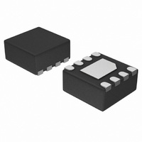
IC MOSFET GATE DVR DUAL 8-DFN

NCP5359AMNR2G

Manufacturer Part Number
NCP5359AMNR2G
Description
IC MOSFET GATE DVR DUAL 8-DFN
Manufacturer
ON Semiconductor
Type
High Side/Low Sider
Datasheet

Specifications of NCP5359AMNR2G

Configuration
High and Low Side, Synchronous
Input Type
PWM
Delay Time
10.0ns
Number Of Configurations
1
Number Of Outputs
2
High Side Voltage - Max (bootstrap)
30V
Voltage - Supply
10 V ~ 13.2 V
Operating Temperature
0°C ~ 85°C
Mounting Type
Surface Mount
Package / Case
8-VFDFN Exposed Pad
Product
MOSFET Gate Drivers
Propagation Delay Time
25 ns
Supply Voltage (max)
15 V
Supply Voltage (min)
- 0.3 V
Maximum Operating Temperature
+ 150 C
Mounting Style
SMD/SMT
Minimum Operating Temperature
0 C
Output Voltage
35 V
Lead Free Status / RoHS Status
Lead free / RoHS Compliant
Current - Peak
-
Lead Free Status / Rohs Status
Lead free / RoHS Compliant

Available stocks

Company
Part Number
Manufacturer
Quantity
Price
Part Number:
NCP5359AMNR2G
Manufacturer:
FREESCALE
Quantity:
101
Part Number:
NCP5359AMNR2G
Manufacturer:
ON/安森美
Quantity:
20 000
Part Number:
NCP5359AMNR2G
Manufacturer:
ON
Quantity:
14 744
NCP5359A
Gate Driver for Notebook
Power Systems
optimized to drive the gates of both high−side and low−side power
MOSFETs in a synchronous buck converter. Each of the drivers can
drive up to 3 nF load with a 25 ns propagation delay and 15 ns
transition time.
provide a low switching loss and high efficiency solution for notebook
and desktop systems.
as high as 35 V, with transient voltages as high as 35 V. Bidirectional
EN pin can provide a fault signal to controller when the gate driver
fault detect under OVP, UVLO occur. Also, an undervoltage lockout
function guarantees the outputs are low when supply voltage is low,
and a thermal shutdown function provides the IC with
overtemperature protection.
Features
Typical Applications
© Semiconductor Components Industries, LLC, 2009
September, 2009 − Rev. 1
The NCP5359A is a high performance dual MOSFET gate driver
Adaptive nonoverlap and power saving operation circuit can
A high floating top driver design can accommodate VBST voltage
Faster Rise and Fall Times
Thermal Shutdown Protection
Adaptive Nonoverlap Circuit
Floating Top Driver Accommodates Boost Voltages of up to 30 V
Output Disable Control Turns Off Both MOSFETs
Complies with VRM 11.1 Specifications
Undervoltage Lockout
Power Saving Operation Under Light Load Conditions
Thermally Enhanced Package
These are Pb−Free Devices
Power Solutions for Desktop and Notebook Systems
1
NCP5359ADR2G
NCP5359AMNR2G
NCP5359AMNTBG
†For information on tape and reel specifications,
including part orientation and tape sizes, please
refer to our Tape and Reel Packaging Specification
Brochure, BRD8011/D.
8
Device
1
1
PWM
ORDERING INFORMATION
BST
V
PWM
EN
BST
CC
V
EN
CC
PIN CONNECTIONS
A = Assembly Location
L = Wafer Lot
Y = Year
W = Work Week
G = Pb−Free Package
AA = Device Code
M = Date Code
G = Pb−Free Package
http://onsemi.com
CASE 506AA
1
MN SUFFIX
1
CASE 751
D SUFFIX
SOIC−8
DFN8
(Top View)
(Pb−Free)
(Pb−Free)
(Pb−Free)
Package
SOIC−8
DFN8
DFN8
Publication Order Number:
8
8
2500 Tape & Reel
3000 Tape & Reel
3000 Tape & Reel
DIAGRAMS
8
1
MARKING
DRVH
SW
GND
DRVL
DRVH
SW
GND
DRVL
Shipping
1
5359A
NCP5359A/D
ALYW
G
4

Related parts for NCP5359AMNR2G

NCP5359AMNR2G Summary of contents

Page 1

... BST PWM (Top View) ORDERING INFORMATION Device Package NCP5359ADR2G SOIC−8 (Pb−Free) NCP5359AMNR2G DFN8 (Pb−Free) NCP5359AMNTBG DFN8 (Pb−Free) †For information on tape and reel specifications, including part orientation and tape sizes, please refer to our Tape and Reel Packaging Specification Brochure, BRD8011/D. 1 MARKING ...

Page 2

VCC ChipEN Fault EN DRVH Comparator PWM > 2 Else = 0 PWM FPWM Comparator 0.8 V < PWM < 2 Else − GND Q ...

Page 3

PWM 13.2 V PIN DESCRIPTION SOIC−8 DFN8 Symbol 1 1 BST 2 2 PWM VCC 5 5 DRVL 6 6 GND DRVH DRVH BST SW PWM ...

Page 4

MAXIMUM RATINGS Rating Thermal Characteristics, Plastic Package Thermal Resistance Junction−to−Air Operating Junction Temperature Range Operating Ambient Temperature Range Storage Temperature Range Moisture Sensitivity Level Stresses exceeding Maximum Ratings may damage the device. Maximum Ratings are stress ratings only. Functional operation ...

Page 5

ELECTRICAL CHARACTERISTICS Characteristics Supply Voltage V Operating Voltage CC Power ON Reset threshold Supply Current V Quiescent Supply Current in Normal CC Operation V Standby Current CC BST Quiescent Supply Current in Normal Operation BST Standby Current Undervoltage Lockout V ...

Page 6

Table 1. DECODER TRUTH TABLE PWM Input Greater than 2.2 V Greater than 0.8 V, but less than 2.2 V Greater than 0.8 V, but less than 2.2 V Less than 0.8 V PWM tpdl DRVL t fDRVL 90% DRVL ...

Page 7

... NCP3418B, but has two additional new features: Bidirection fault detection and multilevel PWM input. When the gate driver works with ON Semiconductor’s NCP5392 controller, it can provide a difference output logic status through multi−level PWM input. For this new feature, higher efficiency can be provided ...

Page 8

... G C SEATING PLANE −Z− 0.25 (0.010 *For additional information on our Pb−Free strategy and soldering details, please download the ON Semiconductor Soldering and Mounting Techniques Reference Manual, SOLDERRM/D. PACKAGE DIMENSIONS SOIC−8 CASE 751−07 ISSUE 0.10 (0.004 SOLDERING FOOTPRINT* 1 ...

Page 9

... Opportunity/Affirmative Action Employer. This literature is subject to all applicable copyright laws and is not for resale in any manner. PUBLICATION ORDERING INFORMATION LITERATURE FULFILLMENT: Literature Distribution Center for ON Semiconductor P.O. Box 5163, Denver, Colorado 80217 USA Phone: 303−675−2175 or 800−344−3860 Toll Free USA/Canada Fax: 303− ...

Related keywords