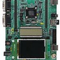
STM32L152-EVAL STMicroelectronics, STM32L152-EVAL Datasheet
STM32L152-EVAL
Specifications of STM32L152-EVAL


Related parts for STM32L152-EVAL


STM32L152-EVAL Summary of contents
Page 1
... STM32L152xx Preliminary data BGA100 7 × BGA64 5 × and USARTs reference with IC/OC/PWM channels window interfaces (SMBus/PMBus) LIN, IrDA capability, modem control) Device summary Part number STM32L151CB, STM32L151RB, STM32L151VB, STM32L151C8, STM32L151R8, STM32L151V8 STM32L152CB, STM32L152RB, STM32L152VB, STM32L152C8, STM32L152R8, STM32L152V8 UFQFPN48 7 × 1/107 www.st.com 1 ...
Page 2
... Performance . . . . . . . . . . . . . . . . . . . . . . . . . . . . . . . . . . . . . . . . . . . . . 11 Shared peripherals . . . . . . . . . . . . . . . . . . . . . . . . . . . . . . . . . . . . . . . . 11 Common system strategy . . . . . . . . . . . . . . . . . . . . . . . . . . . . . . . . . . . 11 Features . . . . . . . . . . . . . . . . . . . . . . . . . . . . . . . . . . . . . . . . . . . . . . . . . 11 Power supply schemes . . . . . . . . . . . . . . . . . . . . . . . . . . . . . . . . . . . . . 15 Power supply supervisor . . . . . . . . . . . . . . . . . . . . . . . . . . . . . . . . . . . . 15 Voltage regulator . . . . . . . . . . . . . . . . . . . . . . . . . . . . . . . . . . . . . . . . . . 15 Boot modes . . . . . . . . . . . . . . . . . . . . . . . . . . . . . . . . . . . . . . . . . . . . . . 15 General-purpose timers (TIM2, TIM3, TIM4, TIM9, TIM10 and TIM11) 21 Basic timers (TIM6 and TIM7 SysTick timer . . . . . . . . . . . . . . . . . . . . . . . . . . . . . . . . . . . . . . . . . . . . . 22 Independent watchdog (IWDG Doc ID 17659 Rev 4 STM32L151xx, STM32L152xx ...
Page 3
... STM32L151xx, STM32L152xx 3.14.5 3.15 Communication interfaces . . . . . . . . . . . . . . . . . . . . . . . . . . . . . . . . . . . . 23 3.15.1 3.15.2 3.15.3 3.15.4 3.16 CRC (cyclic redundancy check) calculation unit . . . . . . . . . . . . . . . . . . . 23 3.17 Development support . . . . . . . . . . . . . . . . . . . . . . . . . . . . . . . . . . . . . . . . 24 4 Pin descriptions . . . . . . . . . . . . . . . . . . . . . . . . . . . . . . . . . . . . . . . . . . . 25 5 Memory mapping . . . . . . . . . . . . . . . . . . . . . . . . . . . . . . . . . . . . . . . . . . 40 6 Electrical characteristics . . . . . . . . . . . . . . . . . . . . . . . . . . . . . . . . . . . . 41 6.1 Parameter conditions . . . . . . . . . . . . . . . . . . . . . . . . . . . . . . . . . . . . . . . . 41 6.1.1 6.1.2 6.1.3 6.1.4 6.1.5 6.1.6 6.1.7 6.2 Absolute maximum ratings . . . . . . . . . . . . . . . . . . . . . . . . . . . . . . . . . . . . 43 6 ...
Page 4
... Package mechanical data . . . . . . . . . . . . . . . . . . . . . . . . . . . . . . . . . . . . 95 7.2 Thermal characteristics . . . . . . . . . . . . . . . . . . . . . . . . . . . . . . . . . . . . . 103 7.2.1 8 Ordering information scheme . . . . . . . . . . . . . . . . . . . . . . . . . . . . . . . 104 9 Revision history . . . . . . . . . . . . . . . . . . . . . . . . . . . . . . . . . . . . . . . . . . 105 4/107 Communications interfaces . . . . . . . . . . . . . . . . . . . . . . . . . . . . . . . . . . 78 12-bit ADC characteristics . . . . . . . . . . . . . . . . . . . . . . . . . . . . . . . . . . . 84 DAC electrical specifications . . . . . . . . . . . . . . . . . . . . . . . . . . . . . . . . . 90 Temperature sensor characteristics . . . . . . . . . . . . . . . . . . . . . . . . . . . . 92 Comparator . . . . . . . . . . . . . . . . . . . . . . . . . . . . . . . . . . . . . . . . . . . . . . 93 LCD controller (STM32L152xx only Reference document . . . . . . . . . . . . . . . . . . . . . . . . . . . . . . . . . . . . . . 103 Doc ID 17659 Rev 4 STM32L151xx, STM32L152xx ...
Page 5
... STM32L151xx, STM32L152xx List of tables Table 1. Device summary . . . . . . . . . . . . . . . . . . . . . . . . . . . . . . . . . . . . . . . . . . . . . . . . . . . . . . . . . . 1 Table 2. Ultralow power STM32L15xxx device features and peripheral counts . . . . . . . . . . . . . . . . 10 Table 3. Timer feature comparison . . . . . . . . . . . . . . . . . . . . . . . . . . . . . . . . . . . . . . . . . . . . . . . . . . 21 Table 4. STM32L15xxx pin definitions . . . . . . . . . . . . . . . . . . . . . . . . . . . . . . . . . . . . . . . . . . . . . . . 30 Table 5. Alternate function input/output . . . . . . . . . . . . . . . . . . . . . . . . . . . . . . . . . . . . . . . . . . . . . . 35 Table 6. Voltage characteristics . . . . . . . . . . . . . . . . . . . . . . . . . . . . . . . . . . . . . . . . . . . . . . . . . . . . 43 Table 7. Current characteristics . . . . . . . . . . . . . . . . . . . . . . . . . . . . . . . . . . . . . . . . . . . . . . . . . . . . 43 Table 8. Thermal characteristics Table 9. General operating conditions . . . . . . . . . . . . . . . . . . . . . . . . . . . . . . . . . . . . . . . . . . . . . . . 44 Table 10 ...
Page 6
... LQPF100 mm, 100-pin low-profile quad flat package mechanical data . . . . . . . 100 Table 61. LQFP64 mm, 64-pin low-profile quad flat package mechanical data . . . . . . . . . 101 Table 62. LQFP48 mm, 48-pin low-profile quad flat package mechanical data . . . . . . . . . . . 102 Table 63. Thermal characteristics 103 Table 64. Ordering information scheme . . . . . . . . . . . . . . . . . . . . . . . . . . . . . . . . . . . . . . . . . . . . . . 104 6/107 = 16 MHz(1 Doc ID 17659 Rev 4 STM32L151xx, STM32L152xx ...
Page 7
... STM32L151xx, STM32L152xx List of figures Figure 1. Ultralow power STM32L15xxx block diagram Figure 2. Clock tree . . . . . . . . . . . . . . . . . . . . . . . . . . . . . . . . . . . . . . . . . . . . . . . . . . . . . . . . . . . . . . 17 Figure 3. STM32L15xxx UFBGA100 ballout . . . . . . . . . . . . . . . . . . . . . . . . . . . . . . . . . . . . . . . . . . . 25 Figure 4. STM32L15xxx TFBGA64 ballout . . . . . . . . . . . . . . . . . . . . . . . . . . . . . . . . . . . . . . . . . . . . 26 Figure 5. STM32L15xxx LQFP100 pinout . . . . . . . . . . . . . . . . . . . . . . . . . . . . . . . . . . . . . . . . . . . . . 27 Figure 6. STM32L15xxx LQFP64 pinout . . . . . . . . . . . . . . . . . . . . . . . . . . . . . . . . . . . . . . . . . . . . . . 28 Figure 7. STM32L15xxx LQFP48 pinout . . . . . . . . . . . . . . . . . . . . . . . . . . . . . . . . . . . . . . . . . . . . . . 28 Figure 8. STM32L15xxx UFQFPN48 pinout . . . . . . . . . . . . . . . . . . . . . . . . . . . . . . . . . . . . . . . . . . . 29 Figure 9. Memory map . . . . . . . . . . . . . . . . . . . . . . . . . . . . . . . . . . . . . . . . . . . . . . . . . . . . . . . . . . . . 40 Figure 10. ...
Page 8
... Introduction This datasheet provides the ordering information and mechanical device characteristics of the STM32L151xx and STM32L152xx ultralow power ARM Cortex™-based microcontrollers product line. The ultralow power STM32L15xxx family includes devices in 3 different package types: from 48 pins to 100 pins. Depending on the device chosen, different sets of peripherals are included, the description below gives an overview of the complete range of peripherals proposed in this family ...
Page 9
... STM32L151xx, STM32L152xx 2 Description The ultralow power STM32L15xxx incorporates the connectivity power of the universal serial bus (USB) with the high-performance ARM Cortex a 32 MHz frequency, a memory protection unit (MPU), high-speed embedded memories (Flash memory up to 128 Kbytes and RAM Kbytes), and an extensive range of enhanced I/Os and peripherals connected to two APB buses ...
Page 10
... Ultralow power STM32L15xxx device features and peripheral counts Peripheral Flash - Kbytes RAM - Kbytes Timers Communication interfaces GPIOs 12-bit synchronized ADC Number of channels 12-bit DAC Number of channels LCD (STM32L152xx Only) COM x SEG Comparator CPU frequency Operating voltage Operating temperatures Packages 10/107 STM32L15xCx 64 10 General-purpose ...
Page 11
... STM32L151xx, STM32L152xx 2.2 Ultralow power device continuum The ultralow power STM32L151xx and STM32L152xx are fully pin-to-pin, software and feature compatible. Besides the full compatibility within the family, the devices are part of STMicroelectronics microcontrollers ultralow power strategy which also includes STM8L101xx and STM8L15xx devices. The STM8L and STM32L families allow a continuum of performance, peripherals, system architecture and features. They are all based on STMicroelectronics 0.13 µ ...
Page 12
... Functional overview 3 Functional overview Figure 1 shows the block diagrams. Figure 1. Ultralow power STM32L15xxx block diagram alternate function on I/O port pin. 12/107 Doc ID 17659 Rev 4 STM32L151xx, STM32L152xx ...
Page 13
... STM32L151xx, STM32L152xx 3.1 Low power modes The ultralow power STM32L15xxx supports dynamic voltage scaling to optimize its power consumption in run mode. The voltage from the internal low-drop regulator that supplies the logic can be adjusted according to the system’s maximum operating frequency and the external voltage supply: ● ...
Page 14
... Processing of late arriving, higher-priority interrupts ● Support for tail-chaining ● Processor state automatically saved ● Interrupt entry restored on interrupt exit with no instruction overhead This hardware block provides flexible interrupt management features with minimal interrupt latency. 14/107 Table 19. Doc ID 17659 Rev 4 STM32L151xx, STM32L152xx ...
Page 15
... STM32L151xx, STM32L152xx 3.3 Reset and supply management 3.3.1 Power supply schemes ● 1.65 to 3.6 V: external power supply for I/Os and the internal regulator. DD Provided externally through V ● SSA DDA and PLL (minimum voltage to be applied and V DDA SSA 3.3.2 Power supply supervisor The device has an integrated ZEROPOWER power-on reset (POR)/power-down reset (PDR) that can be coupled with a brownout reset (BOR) circuitry ...
Page 16
... Several prescalers allow the configuration of the AHB frequency, the high-speed APB (APB2) and the low-speed APB (APB1) domains. The maximum frequency of the AHB and the APB domains is 32 MHz. See 16/107 Figure 2 for details on the clock tree. Doc ID 17659 Rev 4 STM32L151xx, STM32L152xx ...
Page 17
... STM32L151xx, STM32L152xx Figure 2. Clock tree 2. For the USB function to be available, both HSE and PLL must be enabled, with the CPU running at either 24 MHz or 32 MHz. 3.5 Low power real-time clock and backup registers The real-time clock (RTC independent BCD timer/counter. Dedicated registers contain the second, minute, hour (12/24 hour), week day, date, month, year, in BCD (binary-coded decimal) format ...
Page 18
... A pending register maintains the status of the interrupt requests. The EXTI can detect an external line with a pulse width shorter than the Internal APB2 clock period GPIOs can be connected to the 16 external interrupt lines. 18/107 Doc ID 17659 Rev 4 STM32L151xx, STM32L152xx ...
Page 19
... STM32L151xx, STM32L152xx 3.7 Memories The STM32L15xxx devices have the following features: ● Kbyte of embedded RAM accessed (read/write) at CPU clock speed with 0 wait states. With the enhanced bus matrix, operating the RAM does not lead to any performance penalty during accesses to the system bus (AHB and APB buses). ...
Page 20
... V Eight DAC trigger inputs are used in the STM32L15xxx. The DAC channels are triggered through the timer update outputs that are also connected to different DMA channels. 20/107 < 3.6 V. The temperature sensor is internally DDA REF+ Doc ID 17659 Rev 4 STM32L151xx, STM32L152xx ...
Page 21
... STM32L151xx, STM32L152xx 3.12 Ultralow power comparators and reference voltage The STM32L15xxx embeds two comparators sharing the same current bias and reference voltage. The reference voltage can be internal or external (coming from an I/O). ● one comparator with fixed threshold ● one comparator with rail-to-rail inputs, fast or slow mode. The threshold can be one of the following: – ...
Page 22
... The window watchdog is based on a 7-bit downcounter that can be set as free-running. It can be used as a watchdog to reset the device when a problem occurs clocked from the main clock. It has an early warning interrupt capability and the counter can be frozen in debug mode. 22/107 Doc ID 17659 Rev 4 STM32L151xx, STM32L152xx ...
Page 23
... STM32L151xx, STM32L152xx 3.15 Communication interfaces 3.15.1 I²C bus Up to two I²C bus interfaces can operate in multimaster and slave modes. They can support standard and fast modes. They support dual slave addressing (7-bit only) and both 7- and 10-bit addressing in master mode. A hardware CRC generation/verification is embedded. ...
Page 24
... Real-time instruction and data flow activity can be recorded and then formatted for display on the host computer running debugger software. TPA hardware is commercially available from common development tool vendors. It operates with third party debugger software tools. 24/107 Doc ID 17659 Rev 4 STM32L151xx, STM32L152xx ...
Page 25
... STM32L151xx, STM32L152xx 4 Pin descriptions Figure 3. STM32L15xxx UFBGA100 ballout 1 PE3 A B PE4 C PC13 RTC_AF1 WKUP2 D PC14 OSC32_IN E PC15 OSC32_OUT F PH0 OSC_IN G PH1 OSC_OUT H PC0 J VSSA K VREF- L VREF+ M VDDA BOOT0 PD5 PB8 PD7 PE1 PB7 PD6 PB9 PB6 PE2 VDD_3 PB5 PE0 PE5 ...
Page 26
... BOOT0 V SS_4 PB7 PB5 V DD_4 PB6 V SS_3 PC1 PC0 V DD_3 PC2 PA2 PA5 PA0-WKUP1 PA3 PA6 PA1 PA4 PA7 Doc ID 17659 Rev 4 STM32L151xx, STM32L152xx PB3 PA15 PA14 PA13 PD2 PC11 PC10 PA12 PC12 PA10 PA9 PA11 V SS_2 V SS_1 PA8 PC9 V DD_2 ...
Page 27
... STM32L151xx, STM32L152xx Figure 5. STM32L15xxx LQFP100 pinout PE6-WKUP3 PC13-RTC_AF1-WKUP2 PC14-OSC32_IN PC15-OSC32_OUT PH0-OSC_IN PH1-OSC_OUT PA0-WKUP1 PE2 1 PE3 2 PE4 3 PE5 LCD VSS_5 10 VDD_5 NRST 14 PC0 15 PC1 16 PC2 17 PC3 18 VSSA 19 VREF- 20 VREF+ 21 VDDA 22 23 PA1 24 PA2 25 Doc ID 17659 Rev 4 Pin descriptions LQFP100 VDD_2 VSS_2 PH2 ...
Page 28
... PA0-WKUP1 14 PA1 15 PA2 LCD 1 RTC_AF1-WKUP2 2 PC14-OSC32_IN 3 PC15-OSC32_OUT 4 PH0-OSC_IN 5 PH1-OSC_OUT LQFP48 6 NRST 7 VSSA 8 VDDA 9 PA0-WKUP1 10 PA1 11 PA2 Doc ID 17659 Rev 4 STM32L151xx, STM32L152xx 48 VDD_2 47 VSS_2 46 PA13 45 PA12 44 PA11 43 PA10 42 PA9 PA8 41 PC9 40 PC8 39 PC7 38 PC6 37 36 PB15 35 PB14 34 PB13 33 PB12 ai15693b VDD_2 36 VSS_2 ...
Page 29
... STM32L151xx, STM32L152xx Figure 8. STM32L15xxx UFQFPN48 pinout PC13-RTC_AF1 PC14-OSC32_IN PC15-OSC32_OUT PH0-OSC_IN PH1-OSC_OUT PA0-WKUP LCD VFQPN48 7 NRST V 8 SSA V 9 DDA 10 11 PA1 12 PA2 Doc ID 17659 Rev 4 Pin descriptions DD_2 V 35 SS_2 PA13 34 33 PA12 32 PA11 PA10 31 PA9 30 29 PA8 28 PB15 27 PB14 26 PB13 ...
Page 30
... ADC_IN10/LCD_SEG18/ COMP1_INP I/O FT PC1 ADC_IN11/LCD_SEG19/ COMP1_INP I/O FT PC2 ADC_IN12/LCD_SEG20/ COMP1_INP I/O PC3 ADC_IN13/LCD_SEG21/ COMP1_INP S V SSA S V REF REF DDA WKUP1/USART2_CTS/ADC_IN0/TIM2_CH1_ETR/ I/O FT PA0 Doc ID 17659 Rev 4 STM32L151xx, STM32L152xx Alternate functions TRACECK/LCD_SEG38/TIM3_ETR TRACED0/LCD_SEG39/TIM3_CH1 TRACED1/TIM3_CH2 TRACED2/TIM9_CH1 TRACED3/WKUP3/TIM9_CH2 RTC_AF1/WKUP2 OSC32_IN OSC32_OUT OSC_IN OSC_OUT COMP1_INP ...
Page 31
... STM32L151xx, STM32L152xx Table 4. STM32L15xxx pin definitions (continued) Pins Pin name PA1 PA2 PA3 SS_4 DD_4 PA4 PA5 PA6 PA7 PC4 PC5 PB0 PB1 PB2 PE7 PE8 PE9 PE10 PE11 PE12 M10 - PE13 M11 - PE14 M12 - PE15 Main (3) function (after reset) USART2_RTS/ADC_IN1/ TIM2_CH2/LCD_SEG0/ ...
Page 32
... I/O FT PC8 I/O FT PC9 I/O FT PA8 I/O FT PA9 I/O FT PA10 I/O FT PA11 USART1_CTS/ USBDM/SPI1_MISO I/O FT PA12 I/O FT JTMS/SWDIO Doc ID 17659 Rev 4 STM32L151xx, STM32L152xx Alternate functions COMP1_INP/TIM9_CH1 COMP1_INP/TIM9_CH2 USART3_TX/LCD_SEG28 USART3_RX/LCD_SEG29 USART3_CK/LCD_SEG30 USART3_CTS/LCD_SEG31 TIM4_CH1 / USART3_RTS/ LCD_SEG32 TIM4_CH2/LCD_SEG33 TIM4_CH3/LCD_SEG34 TIM4_CH4/LCD_SEG35 TIM3_CH1/LCD_SEG24 TIM3_CH2/LCD_SEG25 TIM3_CH3/LCD_SEG26 TIM3_CH4/LCD_SEG27 ...
Page 33
... STM32L151xx, STM32L152xx Table 4. STM32L15xxx pin definitions (continued) Pins Pin name C11 - PH2 F11 35 V SS_2 G11 36 V DD_2 A10 37 PA14 PA15 B11 - PC10 C10 - PC11 B10 - PC12 PD0 PD1 PD2 PD3 PD4 PD5 PD6 PD7 PB3 PB4 PB5 PB6 PB7 BOOT0 ...
Page 34
... For example device has only one SPI and two USARTs, they will be called SPI1 and USART1 & USART2, respectively. Refer to 4. Applicable to STM32L152xx devices only. In STM32L151xx devices, this pin should be connected The PC14 and PC15 I/Os are only configured as OSC32_IN/OSC32_OUT when the LSE oscillator is on (by setting the LSEON bit in the RCC_CSR register) ...
Page 35
Table 5. Alternate function input/output AFIO0 AFIO1 AFIO2 AFIO3 Port name SYSTEM TIM2 TIM3/4 TIM9/10/11 BOOT0 BOOT0 NRST NRST TIM2_CH1_ PA0-WKUP1 WKUP1 ETR PA1 TIM2_CH2 PA2 TIM2_CH3 TIM9_CH1 PA3 TIM2_CH4 TIM9_CH2 PA4 TIM2_CH1_ PA5 ETR PA6 TIM3_CH1 TIM10_CH1 PA7 TIM3_CH2 ...
Page 36
Table 5. Alternate function input/output (continued) AFIO0 AFIO1 AFIO2 AFIO3 Port name SYSTEM TIM2 TIM3/4 TIM9/10/11 TIM2_CH1_ PA15 JTDI ETR PB0 TIM3_CH3 PB1 TIM3_CH4 PB2 BOOT1 PB3 JTDO TIM2_CH2 PB4 JTRST TIM3_CH1 PB5 TIM3_CH2 PB6 TIM4_CH1 PB7 TIM4_CH2 TIM10_CH1 PB8 ...
Page 37
Table 5. Alternate function input/output (continued) AFIO0 AFIO1 AFIO2 AFIO3 Port name SYSTEM TIM2 TIM3/4 TIM9/10/11 PC1 PC2 PC3 PC4 PC5 PC6 TIM3_CH1 PC7 TIM3_CH2 PC8 TIM3_CH3 PC9 TIM3_CH4 PC10 PC11 PC12 PC13- RTC_AF1 / RTC_AF1 WKUP2 PC14- OSC32_IN OSC32_IN ...
Page 38
Table 5. Alternate function input/output (continued) AFIO0 AFIO1 AFIO2 AFIO3 Port name SYSTEM TIM2 TIM3/4 TIM9/10/11 PD2 TIM3_ETR PD3 PD4 PD5 PD6 PD7 TIM9_CH2 PD8 PD9 PD10 PD11 PD12 TIM4_CH1 PD13 TIM4_CH2 PD14 TIM4_CH3 PD15 TIM4_CH4 PE0 TIM4_ETR TIM10_CH1 PE1 ...
Page 39
Table 5. Alternate function input/output (continued) AFIO0 AFIO1 AFIO2 AFIO3 Port name SYSTEM TIM2 TIM3/4 TIM9/10/11 PE4 TRACED1 TIM3_CH2 PE5 TRACED2 TIM9_CH1* TRACED3 / PE6 TIM9_CH2* WKUP3 PE7 PE8 TIM2_CH1_ PE9 ETR PE10 TIM2_CH2 PE11 TIM2_CH3 PE12 TIM2_CH4 PE13 PE14 ...
Page 40
... Data EEPROM 0x0808 0000 0x0801 FFFF Flash memory Reserved 0x0800 0000 Aliased to Flash or system memory depending on BOOT pins 0x0000 0000 Doc ID 17659 Rev 4 STM32L151xx, STM32L152xx APB memory space 0xFFFF FFFF reserved 0xE010 0000 reserved 0x6000 0000 reserved 0x4002 6400 DMA 0x4002 6000 ...
Page 41
... STM32L151xx, STM32L152xx 6 Electrical characteristics 6.1 Parameter conditions Unless otherwise specified, all voltages are referenced to V 6.1.1 Minimum and maximum values Unless otherwise specified the minimum and maximum values are guaranteed in the worst conditions of ambient temperature, supply voltage and frequencies by tests in production on 100% of the devices with an ambient temperature at T the selected temperature range) ...
Page 42
... Figure 13. Current consumption measurement scheme 42/107 OUT GP I/ DD1/2/.../5 Regulator V SS1/2/.../5 V DDA V REF V REF ADC V REF- V SSA DDA Doc ID 17659 Rev 4 STM32L151xx, STM32L152xx Standby-power circuitry (OSC32K,RTC, Wake-up logic RTC backup registers) IO Logic IN Kernel logic (CPU, Digital & Memories) Analog: RCs, PLL, ... . DD2 ai14126b ai15401c ...
Page 43
... STM32L151xx, STM32L152xx 6.2 Absolute maximum ratings Stresses above the absolute maximum ratings listed in Table 7: Current characteristics, and damage to the device. These are stress ratings only and functional operation of the device at these conditions is not implied. Exposure to maximum rating conditions for extended periods may affect device reliability. ...
Page 44
... V from the same source. A maximum difference of 300 mV DD DDA can be tolerated during power-up and operation. DDA values are allowed as long 103). can be extended to this range as long 103). Doc ID 17659 Rev 4 STM32L151xx, STM32L152xx Value –65 to +150 150 Conditions Min Max 1.65 3 ...
Page 45
... STM32L151xx, STM32L152xx Table 10. Functionalities depending on the operating power supply range Operating power DAC and ADC supply range operation V = 1.65 to 1.8 V Not functional DD Conversion V = 1.8 to 2.0 V time up to 500 DD Conversion V = 2.0 to 2.4 V time up to 500 DD Conversion V = 2.4 to 3.6 V time Msps Functionalities depending on the operating power supply range ...
Page 46
... Reset temporization RSTTEMPO 46/107 Table 9. Conditions BOR detector enabled BOR detector disabled BOR detector enabled BOR detector disabled V rising, BOR enabled DD V rising, BOR disabled DD Doc ID 17659 Rev 4 STM32L151xx, STM32L152xx Min Typ Max Unit 1000 µs/V 1000 2 3.3 ms 0.4 ...
Page 47
... STM32L151xx, STM32L152xx Table 11. Embedded reset and power control block characteristics (continued) Symbol Parameter Power on/power down reset V POR/PDR threshold V Brown-out reset threshold 0 BOR0 V Brown-out reset threshold 1 BOR1 V Brown-out reset threshold 2 BOR2 V Brown-out reset threshold 3 BOR3 V Brown-out reset threshold 4 BOR4 Programmable voltage detector ...
Page 48
... J voltage during Including uncertainties due to ADC and V /V DDA REF+ –40 °C < T < +105 ° °C < T < +50 °C J 1000 hours °C (4) Doc ID 17659 Rev 4 STM32L151xx, STM32L152xx Min Max Typ 1.202 1.224 1.242 1.4 2 2.99 3 3.01 ±5 values 20 50 ...
Page 49
... STM32L151xx, STM32L152xx 6.3.4 Supply current characteristics The current consumption is a function of several parameters and factors such as the operating voltage, ambient temperature, I/O pin loading, device software configuration, operating frequencies, I/O pin switching rate, program location in memory and executed binary code. The current consumption is measured as described in ...
Page 50
... MHz CORE VOS[1: Range MHz CORE VOS[1: kHz Range 3, V =1.2 V 512 kHz CORE VOS[1: MHz Doc ID 17659 Rev 4 STM32L151xx, STM32L152xx (1) Max Typ Unit 55 °C 85 °C 105 °C 200 300 300 300 380 500 500 500 µA (3) 720 860 860 860 0 ...
Page 51
... STM32L151xx, STM32L152xx Table 15. Current consumption in Sleep mode Symbol Parameter HSE = 16 MHz (PLL ON for f >16 MHz) Supply current in Sleep mode, code executed from RAM, Flash switched HSI clock source OFF (16 MHz) MSI clock, 64 kHz I DD MSI clock, 512 kHz (Sleep) MSI clock, 4 MHz ...
Page 52
... T A MSI clock, 64 kHz kHz HCLK MSI clock, 64 kHz kHz HCLK MSI clock, 128 kHz 128 kHz T HCLK Doc ID 17659 Rev 4 STM32L151xx, STM32L152xx Typ = 25° 25° -40 ° ° ° ° 105 ° ° ° -40 ° ° ° ° 105 °C 70 Max ...
Page 53
... STM32L151xx, STM32L152xx Table 17. Current consumption in Low power sleep mode Symbol Parameter Supply current in I (LP DD Low power Sleep) sleep mode Max allowed I Max current in DD (LP Sleep) Low power Sleep mode 1. Based on characterization, not tested in production, unless otherwise specified. Conditions MSI clock, 64 kHz ...
Page 54
... HSI and HSE OFF, independent watchdog and LSI enabled Regulator in LP mode, LSI, HSI and HSE OFF (no independent watchdog) MSI = 4 MHz MSI = 1 MHz MSI = 64 kHz = 25 °C and Doc ID 17659 Rev 4 STM32L151xx, STM32L152xx (1) Typ Max Unit T = -40°C to 25°C 1 55°C 3 85° ...
Page 55
... STM32L151xx, STM32L152xx 3. LCD enabled with external VLCD, 1/4 duty, 1/3 bias, division ratio = 64, all pixels active, no LCD connected. Table 19. Typical and maximum current consumptions in Standby mode Symbol Parameter I DD Supply current in Standby (Standby mode with RTC enabled with RTC) Supply current in Standby ...
Page 56
... HCLK f HCLK f HCLK f HCLK Wakeup from Standby mode f HCLK FWU bit = 1 Wakeup from Standby mode f HCLK FWU bit = °C. A Doc ID 17659 Rev 4 STM32L151xx, STM32L152xx supply DD (1) Conditions Typ Max Unit = 32 MHz 0.36 = 128 kHz 32 = 128 kHz 4.2 MHz TBD MSI = f = 4.2 MHz MSI 8 ...
Page 57
... STM32L151xx, STM32L152xx On-chip peripheral current consumption The current consumption of the on-chip peripherals is given in the following table. The MCU is placed under the following conditions: ● all I/O pins are in input mode with a static value at V ● all peripherals are disabled unless otherwise mentioned ● ...
Page 58
... OFF an one peripheral with clock MHz (range 1), f HCLK = f APB1 measurement between ADC in reset configuration and continuous ADC DD Doc ID 17659 Rev 4 STM32L151xx, STM32L152xx (continued ° Range Low power CORE 1.2 V sleep and VOS[1:0] = run ...
Page 59
... STM32L151xx, STM32L152xx 4. Data based on a differential I conversion Including supply current of internal reference voltage. 6.3.5 External clock source characteristics High-speed external user clock generated from an external source The characteristics given in external clock source, and under ambient temperature and supply voltage conditions summarized in Table Table 22 ...
Page 60
... I OSC32_IN Input leakage current L 1. Guaranteed by design, not tested in production. Figure 14. Low-speed external clock source AC timing diagram 60/107 9. Parameter Conditions (1) (1) (1) (1) Doc ID 17659 Rev 4 STM32L151xx, STM32L152xx Min Typ Max 1 32.768 1000 0. 0.3V SS TBD TBD 0.6 TBD TBD V ...
Page 61
... STM32L151xx, STM32L152xx Figure 15. High-speed external clock source AC timing diagram High-speed external clock generated from a crystal/ceramic resonator The high-speed external (HSE) clock can be supplied with MHz crystal/ceramic resonator oscillator. All the information given in this paragraph are based on characterization results obtained with typical external components specified in the resonator and the load capacitors have to be placed as close as possible to the oscillator pins in order to minimize output distortion and startup stabilization time ...
Page 62
... with 30 pF load MHz OSC MHz OSC Startup V is stabilized DD and C . PCB and MCU pin capacitance must be included ( Doc ID 17659 Rev 4 STM32L151xx, STM32L152xx (1)(2) Min Typ Max 1 24 200 2.5 (startup) 0.7 (stabilized) 2.5 (startup) 0.46 (stabilized) 3.5 1 Figure 16). C and C ...
Page 63
... STM32L151xx, STM32L152xx Figure 16. HSE oscillator circuit diagram 1. R value depends on the crystal characteristics. EXT Low-speed external clock generated from a crystal/ceramic resonator The low-speed external (LSE) clock can be supplied with a 32.768 kHz crystal/ceramic resonator oscillator. All the information given in this paragraph are based on characterization ...
Page 64
... Example: if you choose a resonator with a load capacitance of C then pF Figure 17. Typical application with a 32.768 kHz crystal 64/107 L1 has the following formula and C L1 7 pF. Never use a resonator with a load L Doc ID 17659 Rev 4 STM32L151xx, STM32L152xx Figure and stray (15 pF strongly recommended L2 ...
Page 65
... STM32L151xx, STM32L152xx 6.3.6 Internal clock source characteristics The parameters given in temperature and V High-speed internal (HSI) RC oscillator Table 26. HSI oscillator characteristics Symbol Parameter f Frequency HSI HSI user-trimmed (2) TRIM resolution Accuracy of the (3) ACC factory-calibrated HSI HSI oscillator HSI oscillator (3) t SU(HSI) startup time ...
Page 66
... Parameter = 25 °C A (2) 85 °C A (2) 3 ° (2) 1 ° Doc ID 17659 Rev 4 STM32L151xx, STM32L152xx Condition Typ Max Unit MSI range 0 65.5 MSI range 1 131 MSI range 2 262 = DD MSI range 3 524 MSI range 4 1.05 MSI range 5 2.1 MSI range 6 4.2 ...
Page 67
... STM32L151xx, STM32L152xx Table 28. MSI oscillator characteristics Symbol t MSI oscillator startup time SU(MSI) t MSI oscillator stabilization time STAB(MSI) f MSI oscillator frequency overshoot OVER(MSI) 1. 1. This is a deviation for an individual part, once the initial frequency has been measured. 3. Based on characterization, not tested in production. ...
Page 68
... Take care of using the appropriate multiplier factors have PLL input clock values compatible with the range defined by f 68/107 Table 29 are derived from tests performed under ambient supply voltage conditions summarized in DD Parameter (2) DDA DD . PLL_OUT Doc ID 17659 Rev 4 STM32L151xx, STM32L152xx Table 9. Value (1) Min Typ Max ...
Page 69
... STM32L151xx, STM32L152xx 6.3.8 Memory characteristics The characteristics are given at T RAM memory Table 30. RAM and hardware registers Symbol Parameter VRM Data retention mode 1. Minimum supply voltage without losing data stored in RAM (in Stop mode or under Reset hardware registers (only in Stop mode). Guaranteed by technology characteristics, not tested in production. ...
Page 70
... They are based on the EMS levels and classes Parameter HCLK conforms to IEC 61000-4 and HCLK conforms to IEC 61000-4-4 Doc ID 17659 Rev 4 STM32L151xx, STM32L152xx and DD Conditions 3.3 V, LQFP100, T +25 °C, A 32 MHz 3.3 V, LQFP100, T +25 °C, A 32 MHz Level/ Class 2B 4A ...
Page 71
... STM32L151xx, STM32L152xx Prequalification trials Most of the common failures (unexpected reset and program counter corruption) can be reproduced by manually forcing a low state on the NRST pin or the oscillator pins for 1 second. To complete these trials, ESD stress can be applied directly on the device, over the range of specification values ...
Page 72
... CMOS ports CMOS ports CMOS ports Doc ID 17659 Rev 4 STM32L151xx, STM32L152xx Conditions Table 37 are derived from tests Table 9. All I/Os are CMOS and TTL Min Typ Max V - 0.3 0 5.5V –0.3 0 5.25 (2) ...
Page 73
... STM32L151xx, STM32L152xx Table 37. I/O static characteristics (continued) Symbol Parameter (6) I Input leakage current lkg R Weak pull-up equivalent resistor PU R Weak pull-down equivalent resistor PD C I/O pin capacitance tolerant. To sustain a voltage higher than V 2. 0.7V for 5V-tolerant receiver Five-volt tolerant. 4. Hysteresis voltage between Schmitt trigger switching levels. Based on characterization, not tested in production. ...
Page 74
... Based on characterization data, not tested in production. 74/107 Parameter 2.7 V < V 1.65 V < V 2.7 V < V (I/O ports and control pins) must not exceed I (I/O ports and control pins) must not exceed I IO Doc ID 17659 Rev 4 STM32L151xx, STM32L152xx Conditions Min Max 0 < 3 2.4 ...
Page 75
... STM32L151xx, STM32L152xx Input/output AC characteristics The definition and values of input/output AC characteristics are given in Table 39, respectively. Unless otherwise specified, the parameters given in performed under ambient temperature and V Table 9. Table 39. I/O AC characteristics OSPEEDRx [1:0] bit Symbol (1) value f Maximum frequency max(IO)out 00 t f(IO)out Output rise and fall time ...
Page 76
... DD Parameter Conditions I OL 2.7 V < 1 1.65 V < (3) IN Doc ID 17659 Rev 4 STM32L151xx, STM32L152xx 90% t r(I O)out ai14131 Table 40 are derived from tests Min Typ Max Unit < 3 < 2 (2) 10%V DD ...
Page 77
... STM32L151xx, STM32L152xx Figure 19. Recommended NRST pin protection 1. The reset network protects the device against parasitic resets. 2. The user must ensure that the level on the NRST pin can go below the V Table 40. Otherwise the reset will not be taken into account by the device. 6.3.13 TIM timer characteristics The parameters given in the following table are guaranteed by design ...
Page 78
... PCLK1 9. Table 42. Refer also to Standard mode I Parameter Min 4.7 4.0 250 (3) 0 4.0 4.7 4.0 4.7 Doc ID 17659 Rev 4 STM32L151xx, STM32L152xx Table 42 are derived from tests supply voltage conditions communication protocol is disabled, DD Section 6.3.11: I/O port 2 (1) 2 (1)(2) C Fast mode I C ...
Page 79
... STM32L151xx, STM32L152xx 2 Figure 20 bus AC waveforms and measurement circuit 1. Measurement points are done at CMOS levels: 0.3V Table 43. SCL frequency ( External pull-up resistance For speeds around 200 kHz, the tolerance on the achieved speed is of 5%. For other speed ranges, the tolerance on the achieved speed is 2%. These variations depend on the accuracy of the external components used to design the application ...
Page 80
... Master mode Slave mode Slave mode, f Slave mode Slave mode (after enable edge) Master mode (after enable edge) Slave mode (after enable edge) Master mode (after enable edge) Doc ID 17659 Rev 4 STM32L151xx, STM32L152xx frequency and V supply voltage DD Min Max 16 16 TBD ...
Page 81
... STM32L151xx, STM32L152xx Figure 21. SPI timing diagram - slave mode and CPHA = 0 NSS input t SU(NSS) CPHA= 0 CPOL=0 t w(SCKH) CPHA w(SCKL) CPOL=1 t a(SO) MISO OUT su(SI) MOSI I NPUT Figure 22. SPI timing diagram - slave mode and CPHA = 1 NSS input t SU(NSS) CPHA=1 CPOL=0 t w(SCKH) CPHA=1 t w(SCKL) ...
Page 82
... USB startup time Symbol (1) t STARTUP 1. Guaranteed by design, not tested in production. 82/107 t c(SCK) t w(SCKH) t w(SCKL) MS BIN t h(MI OUT OUT t v(MO) and 0.7V DD Parameter USB transceiver startup time Doc ID 17659 Rev 4 STM32L151xx, STM32L152xx (1) t r(SCK) t f(SCK LSB IN LSB OUT t h(MO Max 1 ai14136 Unit µs ...
Page 83
... STM32L151xx, STM32L152xx Table 46. USB DC electrical characteristics Symbol Input levels V USB operating voltage DD (4) V Differential input sensitivity DI (4) V Differential common mode range Includes V CM (4) V Single ended receiver threshold SE Output levels V Static output level low OL V Static output level high OH 1. All the voltages are measured from the local ground potential. ...
Page 84
... DDA input DDA Peak input REF Average (2) Direct channels Multiplexed channels Direct channels Multiplexed channels Direct channels Multiplexed channels Direct channels Multiplexed channels Doc ID 17659 Rev 4 STM32L151xx, STM32L152xx Table 49 are guaranteed by design. Min Max REF+ = DDA REF+ DDA 8 V > 2.4 V REF+ ...
Page 85
... STM32L151xx, STM32L152xx Table 49. ADC characteristics (continued) Symbol t Sampling time S Total conversion time t CONV (including sampling time) Internal sample and hold C ADC capacitor External trigger frequency f TRIG Regular sequencer External trigger frequency f TRIG Injected sequencer (5) R External input impedance AIN Injection trigger conversion ...
Page 86
... DDA 1.8 V V REF MHz, R ADC = -40 to 105 1.8 V V DDA 1.8 V V REF MHz, R ADC = -40 to 105 Doc ID 17659 Rev 4 STM32L151xx, STM32L152xx Typ Max 2 4 3 3.6 V 1.5 3 AIN ±TBD 3 ± ...
Page 87
... STM32L151xx, STM32L152xx Figure 25. ADC accuracy characteristics [1LSB IDEAL 4095 4094 4093 SSA Figure 26. Typical connection diagram using the ADC 1. Refer to Table represents the capacitance of the PCB (dependent on soldering and PCB layout quality) plus the parasitic pad capacitance (roughly 7 pF). A high C this, f should be reduced ...
Page 88
... V 2.4 V < V DDA Not allowed Not allowed 0.8 1.8 4.0 10.0 25.0 50.0 is connected to V REF+ DDA Doc ID 17659 Rev 4 STM32L151xx, STM32L152xx supply pin during ADC REF+ Direct channels < 3.3 V 1.8 V < V DDA DDA 0.7 Not allowed 2.0 1.0 4.0 3.0 6 ...
Page 89
... STM32L151xx, STM32L152xx Figure 28. Power supply and reference decoupling ( and V REF+ REF– Figure 29. Power supply and reference decoupling ( and V REF+ REF– inputs are available only on 100-pin packages. inputs are available only on 100-pin packages. Doc ID 17659 Rev 4 Electrical characteristics V not connected to ...
Page 90
... DAC output buffer ON LOAD L DAC output buffer OFF LOAD L (6) DAC output buffer OFF Doc ID 17659 Rev 4 STM32L151xx, STM32L152xx Min Typ Max 1.8 3.6 1.8 3.6 DDA V SSA 130 220 220 350 210 320 320 520 ...
Page 91
... STM32L151xx, STM32L152xx Table 52. DAC characteristics (continued) Symbol Parameter (1) (7) Gain Gain error (1) TUE Total unadjusted error Settling time (full scale: for a 12-bit code transition between the t lowest and the highest SETTLING input codes till DAC_OUT reaches final value ±1LSB Max frequency for a ...
Page 92
... Shortest sampling time can be determined in the application by multiple iterations. 92/107 Buffer(1) 12-bit DACx_OUT digital to analog converter Parameter linearity with temperature ( ±10 mV. V90 ADC conversion result is stored in the TS_Factory_CONV_V90 byte. Doc ID 17659 Rev 4 STM32L151xx, STM32L152xx R LOAD C LOAD ai17157 Min Typ Max 1 2 1.59 1.62 1.65 mV/° ...
Page 93
... STM32L151xx, STM32L152xx 6.3.18 Comparator Table 54. Comparator 1 characteristics Symbol V Analog supply voltage DDA R R 400K 400K R R 10K 10K V Comparator 1 input voltage range IN t Comparator startup time START td Propagation delay Voffset Comparator offset error I Current consumption COMP1 1. Based on characterization, not tested in production. ...
Page 94
... Electrical characteristics 6.3.19 LCD controller (STM32L152xx only) The STM32L152xx embeds a built-in step-up converter to provide a constant LCD reference voltage independently from the V to the V pin to decouple this converter. LCD Table 56. LCD controller characteristics Symbol V LCD external voltage LCD V LCD internal reference voltage 0 ...
Page 95
... STM32L151xx, STM32L152xx 7 Package characteristics 7.1 Package mechanical data In order to meet environmental requirements, ST offers these devices in different grades of ® ECOPACK packages, depending on their level of environmental compliance. ECOPACK specification s, grade definitions and product status are available at: www.st.com. ® ECOPACK trademark. Doc ID 17659 Rev 4 Package characteristics ® ...
Page 96
... Doc ID 17659 Rev 4 STM32L151xx, STM32L152xx Figure 32. Recommended footprint (dimensions in mm) 7. 6.20 0.20 7.30 6.20 5.60 5.60 0. 0.50 5.80 0.55 (1) inches Typ Min 0 ...
Page 97
... STM32L151xx, STM32L152xx Figure 33. TFBGA64 - active ball array mm, 0.5 mm pitch, package outline Seating plane 1. Drawing is not to scale. Table 58. TFBGA64 - active ball array mm, 0.5 mm pitch, package mechanical data Symbol ddd eee fff 1. Values in inches are converted from mm and rounded to 4 decimal digits ball pad corner ...
Page 98
... Figure 34. Recommended PCB design rules for pads (0.5 mm pitch BGA) Dpad Dsm 1. Non solder mask defined (NSMD) pads are recommended mils solder paste screen printing process 98/107 Pitch 0 pad 0.27 mm 0.35 mm typ (depends on Dsm the soldermask registration tolerance) Solder paste 0.27 mm aperture diameter Doc ID 17659 Rev 4 STM32L151xx, STM32L152xx ai15495 ...
Page 99
... STM32L151xx, STM32L152xx Figure 35. UFBGA100 - ultra fine pitch ball grid array mm, 0.50 mm pitch, package outline A1 ball pad corner 1.75 1. Drawing is not to scale. Table 59. UFBGA100 - ultra fine pitch ball grid array mm, 0.50 mm pitch, package mechanical data Symbol Min A 0.46 A1 0.06 A2 0 Values in inches are converted from mm and rounded to 4 decimal digits. ...
Page 100
... Doc ID 17659 Rev 4 STM32L151xx, STM32L152xx Figure 37. Recommended footprint 75 76 0.5 16.7 14.3 100 1 12.3 16.7 (1) inches Min Typ 0.002 0.0531 0.0551 0.0067 0.0087 0.0035 0.622 ...
Page 101
... STM32L151xx, STM32L152xx Figure 38. LQFP64 mm, 64-pin low-profile quad flat package outline Drawing is not to scale. 2. Dimensions are in millimeters. Table 61. LQFP64 mm, 64-pin low-profile quad flat package mechanical data Symbol Min A A1 0.05 A2 1.35 b 0. 0° Values in inches are converted from mm and rounded to 4 decimal digits. ...
Page 102
... Doc ID 17659 Rev 4 STM32L151xx, STM32L152xx Figure 41. Recommended (1)(2) footprint 0.20 7.30 5.80 9.70 7. 5.80 9.70 (1) inches Typ Min 0.0020 0.0551 ...
Page 103
... STM32L151xx, STM32L152xx 7.2 Thermal characteristics The maximum chip-junction temperature, T using the following equation: Where: max is the maximum ambient temperature in C, ● is the package junction-to-ambient thermal resistance, in C/W, ● JA ● P max is the sum ● P max is the product of I INT internal power. ...
Page 104
... TR = tape and reel No character = tray or tube For a list of available options (speed, package, etc.) or for further information on any aspect of this device, please contact your nearest ST sales office. 104/107 STM32 range: 1.8 to 3.6 V and BOR enabled Doc ID 17659 Rev 4 STM32L151xx, STM32L152xx L 151 xxx ...
Page 105
... STM32L151xx, STM32L152xx 9 Revision history on Table 65. Document revision history Date Revision 02-Jul-2010 01-Oct-2010 16-Dec-2010 25-Feb-2011 1 Initial release. Removed 5 V tolerance (FT) from PA3, PB0 and PC3 in STM32L15xxx pin definitions on page 30 Updated Table 11: Embedded reset and power control block characteristics on page 46 2 Updated Table 12: Embedded internal reference voltage on page 48 ...
Page 106
... Figure 28: Power supply and reference decoupling (VREF+ not connected to VDDA): replaced all 10 nF capacitors with 100 nF capacitors. Figure 29: Power supply and reference decoupling (VREF+ connected to VDDA): replaced 10 nF capacitor with 100 nF capacitor. Doc ID 17659 Rev 4 STM32L151xx, STM32L152xx Changes (WU from Stop). DD modes: updated . WUSTDBY consumption: updated values for column value ...
Page 107
... STM32L151xx, STM32L152xx Information in this document is provided solely in connection with ST products. STMicroelectronics NV and its subsidiaries (“ST”) reserve the right to make changes, corrections, modifications or improvements, to this document, and the products and services described herein at any time, without notice. All ST products are sold pursuant to ST’s terms and conditions of sale. ...