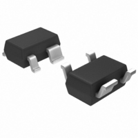
MGA-53543-TR1G Avago Technologies US Inc., MGA-53543-TR1G Datasheet - Page 8

MGA-53543-TR1G
Manufacturer Part Number
MGA-53543-TR1G
Description
IC AMP RFIC 1.9GHZ SOT-343
Manufacturer
Avago Technologies US Inc.
Datasheet
1.MGA-53543-TR1G.pdf
(14 pages)
Specifications of MGA-53543-TR1G
Gain
14dB ~ 17dB
Rf Type
Cellular, PCS
Current - Supply
40mA ~ 70mA
Frequency
0Hz ~ 2.4GHz
Noise Figure
1.5dB ~ 1.9dB
P1db
18.6dBm
Package / Case
SC-70-4, SC-82-4, SOT-323-4, SOT-343
Test Frequency
1.9GHz
Voltage - Supply
5V ~ 5.5V
Frequency Range
50MHz To 6GHz
Noise Figure Typ
1.5dB
Power Dissipation Pd
400mW
Supply Current
54mA
Supply Voltage Range
5V
Manufacturer's Type
Linear Amplifier
Number Of Channels
1
Frequency (max)
6GHz
Operating Supply Voltage (max)
5.5V
Package Type
SOT-343
Mounting
Surface Mount
Pin Count
3 +Tab
Noise Figure (typ)
1.9@2400MHzdB
Lead Free Status / RoHS Status
Lead free / RoHS Compliant
Lead Free Status / RoHS Status
Lead free / RoHS Compliant, Lead free / RoHS Compliant
Other names
516-1826-2
MGA-53543-TR1G
MGA-53543-TR1G
Available stocks
Company
Part Number
Manufacturer
Quantity
Price
Company:
Part Number:
MGA-53543-TR1G
Manufacturer:
AVAGO
Quantity:
15 600
Company:
Part Number:
MGA-53543-TR1G
Manufacturer:
AVAGO
Quantity:
11 800
Part Number:
MGA-53543-TR1G
Manufacturer:
AVAGO/安华高
Quantity:
20 000
RF Grounding
Adequate grounding of Pins 1 and 4 of the RFIC are impor-
tant to maintain device stability and RF performance. Each
of the ground pins should be connected to the ground
plane on the backside of the PCB by means of plated
through holes (vias). The ground vias should be placed as
close to the package terminals as practical to reduce induc-
tance in ground path. It is good practice to use multiple
vias to further minimize ground path inductance.
PCB Materials
FR-4 or G-10 type material is a good choice for most low
cost wireless applications using single or multi-layer
printed circuit boards. Typical single-layer board thickness
is 0.00 to 0.031 inches. Circuit boards thicker than 0.031
inches are not recommended due to excessive inductance
in the ground vias.
For noise figure critical or higher frequency applications,
the additional cost of PTFE/glass dielectric materials may
be warranted to minimize transmission line loss at the
amplifier’s input.
Application Example
The demonstration circuit board for the MGA-53543 is
shown in Figure 16. This simple two-layer board contains
microstripline on the topside and a solid metal ground
plane on the backside with all RF traces having charac-
teristic impedance of 50Ω. Multiple 0.0" vias are used
to bring the ground to the topside of the board and help
reduce ground inductance.
The PCB is fabricated on 0.031" thick Getek® GR00D
dielectric material with dielectric constant of 4..
Figure 16. MGA-53453 PCB Layout.
8
SE
IN
12/01
OUT
Vd
MGA - 5X
1900 MHz HLA Design
The following describes a typical application for the MGA-
53543 as used in a PCS 1900 MHz band radio receiver
optimized for maximum linearity. Steps include matching
the input and output as well as providing a DC bias while
maintaining acceptable stability, gain and noise figure.
As described earlier, a pure linearity match entails match-
ing only to Γ
This tradeoff is explained below and quantified in Figures
8 and 9.
Using the device S-parameters at 1900 MHz, the minimum
noise figure possible, whilst matching the input to Γ
shown to be 1.7 dB.
NF = 1.7 dB
Figure 17. Noise figure performance.
Because gain depends both on the input and output
match, the maximum gain is taken from two sets of circles.
One is centered around S11 and the other is centered on
S. Thus the maximum attainable gain is the lesser of two
circles which completely enclose Γ
Figure 18 the 16.1 dB input gain circle completely encloses
Γ
the maximum gain is the weakest link or 15.9 dB.
Ga = 16.2 dB
Figure 18. Input and output gain circles.
NF = 1.6 dB
NF = 1.5 dB
s
, but the smallest circle that encloses Γ
Figure 9. Input and Output Gain Circles.
Figure 8. Noise figure performance.
Ga = 16.1 dB
Γ
S
s
and Γ
S11
Ga = 15.9 dB
Γ
Γ
S – Optimum linearity match
L
Γ
L
, thus sacrificing some NF and Gain.
opt – Optimum NF match
S22
Ga = 16.1 dB
Ga = 16.2 dB
s
or Γ
L
. For example, in
L
is 15.9 dB. Thus
S
, is


