ADL5542ACPZ-R7 Analog Devices Inc, ADL5542ACPZ-R7 Datasheet - Page 10
ADL5542ACPZ-R7
Manufacturer Part Number
ADL5542ACPZ-R7
Description
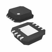
IC GAIN BLOCK 6GHZ 20DB 8LFCSP
Manufacturer
Analog Devices Inc
Datasheet
1.ADL5542ACPZ-R7.pdf
(12 pages)
Specifications of ADL5542ACPZ-R7
Gain
11.2dB ~ 14.4dB
Rf Type
Cellular, CATV
Current - Supply
93mA ~ 115mA
Frequency
50MHz ~ 6GHz
Noise Figure
5.7dB ~ 6.3dB
P1db
6.8dBm
Package / Case
8-LFCSP
Test Frequency
5.8GHz
Voltage - Supply
4.5V ~ 5.5V
Frequency Range
50MHz To 6000MHz
Noise Figure Typ
5.7dB
Power Dissipation Pd
500mW
Supply Current
92mA
Supply Voltage Range
4.5V To 5.5V
Lead Free Status / RoHS Status
Lead free / RoHS Compliant
Lead Free Status / RoHS Status
Lead free / RoHS Compliant, Lead free / RoHS Compliant
Other names
ADL5542ACPZ-R7
ADL5542ACPZ-R7TR
Q3394642A
ADL5542ACPZ-R7TR
Q3394642A
Available stocks
Company
Part Number
Manufacturer
Quantity
Price

Part Number:
ADL5542ACPZ-R7
Manufacturer:
ADI/亚德诺
Quantity:
20 000


ADL5542
BASIC CONNECTIONS
The basic connections for operating the ADL5542 are shown in
Figure 13. Recommended components are listed in Table 5. The
input and output should be ac-coupled with appropriately sized
capacitors (device characterization was performed with 33 pF
capacitors). A 5 V dc bias is supplied to the amplifier via VPOS
(Pin 5) and through a biasing inductor connected to RFOUT
(Pin 8). The bias voltage should be decoupled using a 1 μF
capacitor, a 1.2 nF capacitor, and two 68 pF capacitors.
For operation between 50 MHz and 500 MHz, a larger biasing
choke and ac coupling capacitors are necessary (see Table 5).
Figure 14 shows a plot of the input return loss, the output
return loss, and the gain with these components. At 100 MHz,
the ADL5542 achieves an OIP3 of 38 dBm (P
tone). The noise figure performance for operation from 50 MHz
to 500 MHz is shown in Figure 15. When operating below
50 MHz, the ADL5542 exhibits gain peaking, and the input
and output match degrade significantly.
Table 5. Recommended Components for Basic Connections
Frequency
50 MHz to 500 MHz
500 MHz to 6000 MHz
RFIN
21.0
20.5
20.0
19.5
19.0
18.5
18.0
Figure 14. Input Return Loss (S11), Output Return Loss (S22), and
50
VCC
100
33pF
1µF
C1
C3
150
C6
1µF
Figure 13. Basic Connections
1 RFIN
2 GND
3 GND
4 CB
Gain (S21) vs. Frequency
200
ADL5542
FREQUENCY (MHz)
S21
S11
S22
C1
0.1 μF
33 pF
C5
1.2nF
RFOUT
250
VPOS
GND
GND
300
8
7
6
5
C2
0.1 μF
33 pF
C4
68pF
350
C7
68pF
L1
47nH
VCC
400
GND
OUT
C3
1 μF
1 μF
33pF
C2
= 0 dBm per
450
L1
470 nH (Coilcraft 0603LS-471NXJL_ or equivalent)
47 nH (Coilcraft 0603CS-47NXJL_ or equivalent)
500
10
0
–10
–20
–30
–40
–50
RFOUT
Rev. A | Page 10 of 12
SOLDERING INFORMATION AND RECOMMENDED
PCB LAND PATTERN
Figure 16 shows the recommended land pattern for the ADL5542.
To minimize thermal impedance, the exposed paddle on the
package underside should be soldered down to a ground plane
along with Pin 2, Pin 3, Pin 6, and Pin 7. If multiple ground
layers exist, they should be stitched together using vias (a
minimum of five vias is recommended). For more information
on land pattern design and layout, refer to Application Note
AN-772, A Design and Manufacturing Guide for the Lead Frame
Chip Scale Package (LFCSP).
0.5mm
4.0
3.5
3.0
2.5
2.0
1.5
50
0.71mm
PIN 1
PIN 4
100
Figure 16. Recommended Land Pattern
Figure 15. Noise Figure vs. Frequency
150
200
FREQUENCY (MHz)
2.03mm
1.53mm
250
C4
68 pF
68 pF
1.85mm
300
350
C5
1.2 nF
1.2 nF
PIN 8
PIN 5
400
C6
1 μF
1 μF
450
1.78mm
500
C7
68 pF
68 pF
Related parts for ADL5542ACPZ-R7
Image
Part Number
Description
Manufacturer
Datasheet
Request
R

Part Number:
Description:
±1.7g Dual-Axis IMEMS Accelerometer Evaluation Board
Manufacturer:
Analog Devices Inc
Datasheet:

Part Number:
Description:
Inertial Sensor Evaluation System
Manufacturer:
Analog Devices Inc
Datasheet:
Part Number:
Description:
Manufacturer:
Analog Devices Inc
Datasheet:
Part Number:
Description:
Manufacturer:
Analog Devices Inc
Datasheet:
Part Number:
Description:
Manufacturer:
Analog Devices Inc
Datasheet:
Part Number:
Description:
Manufacturer:
Analog Devices Inc
Datasheet:
Part Number:
Description:
Manufacturer:
Analog Devices Inc
Datasheet:
Part Number:
Description:
Manufacturer:
Analog Devices Inc
Datasheet:
Part Number:
Description:
Manufacturer:
Analog Devices Inc
Datasheet:
Part Number:
Description:
Manufacturer:
Analog Devices Inc
Datasheet:
Part Number:
Description:
Manufacturer:
Analog Devices Inc
Datasheet:
Part Number:
Description:
Manufacturer:
Analog Devices Inc
Datasheet:
Part Number:
Description:
Manufacturer:
Analog Devices Inc
Datasheet: