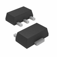
ADL5601ARKZ-R7 Analog Devices Inc, ADL5601ARKZ-R7 Datasheet - Page 11

ADL5601ARKZ-R7
Manufacturer Part Number
ADL5601ARKZ-R7
Description
IC AMP GAIN BLOCK 15DB SOT89-3
Manufacturer
Analog Devices Inc
Datasheet
1.ADL5601ARKZ-R7.pdf
(16 pages)
Specifications of ADL5601ARKZ-R7
Gain
15dB
Current - Supply
83mA
Frequency
50MHz ~ 4GHz
Noise Figure
3.7dB
P1db
19dBm
Package / Case
SC-62, SOT-89, TO-243 (3 Leads + Tab)
Rf Type
General Purpose
Test Frequency
900MHz
Voltage - Supply
4.5 V ~ 5.5 V
Frequency Range
50MHz To 4GHz
Noise Figure Typ
3.9dB
Power Dissipation Pd
420mW
Supply Current
83mA
Supply Voltage Range
4.5V To 5.5V
Rf Ic Case Style
SOT-89
No. Of Pins
3
Lead Free Status / RoHS Status
Lead free / RoHS Compliant
Other names
ADL5601ARKZ-R7
ADL5601ARKZ-R7TR
ADL5601ARKZ-R7TR
Available stocks
Company
Part Number
Manufacturer
Quantity
Price
Company:
Part Number:
ADL5601ARKZ-R7
Manufacturer:
Panasonic
Quantity:
2 988
BASIC CONNECTIONS
The basic connections for operating the ADL5601 are shown in
Figure 15. Recommended components are listed in Table 5. The
input and output should be ac-coupled with appropriately sized
capacitors (the device characterization was performed with
0.1 μF capacitors). A 5 V dc bias is supplied to the amplifier
through the bias inductor connected to RFOUT (Pin 3). The
bias voltage should be decoupled using a 1 μF capacitor, a 1.2 nF
capacitor, and a 68 pF capacitor.
RFIN
Table 5. Recommended Components for Basic Connections
Frequency
50 MHz to 4000 MHz
0.1µF
C1
1
RFIN
GND
ADL5601
(2)
2
Figure 15. Basic Connections
GND
C1
0.1 μF
3
RFOUT
GND
VCC
C2
0.1 μF
L1
470nH
1.2nF
68pF
1µF
C6
C5
C4
0.1µF
C2
L1
470 nH (Coilcraft 0603LS-NX or equivalent)
RFOUT
Rev. 0 | Page 11 of 16
SOLDERING INFORMATION AND RECOMMENDED
PCB LAND PATTERN
Figure 16 shows the recommended land pattern for the ADL5601.
To minimize thermal impedance, the exposed paddle on the
package underside, along with Pin 2, should be soldered to a
ground plane. If multiple ground layers exist, they should be
stitched together using vias. For more information on land
pattern design and layout, refer to the AN-772 Application
Note, A Design and Manufacturing Guide for the Lead Frame
Chip Scale Package (LFCSP).
5.56mm
0.86mm
Figure 16. Recommended Land Pattern
0.20mm
1.50mm
3.00mm
1.80mm
C4
68 pF
3.48mm
C5
1.2 nF
0.62mm
1.27mm
ADL5601
C6
1 μF


