ADL5601ARKZ-R7 Analog Devices Inc, ADL5601ARKZ-R7 Datasheet - Page 8
ADL5601ARKZ-R7
Manufacturer Part Number
ADL5601ARKZ-R7
Description
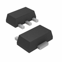
IC AMP GAIN BLOCK 15DB SOT89-3
Manufacturer
Analog Devices Inc
Datasheet
1.ADL5601ARKZ-R7.pdf
(16 pages)
Specifications of ADL5601ARKZ-R7
Gain
15dB
Current - Supply
83mA
Frequency
50MHz ~ 4GHz
Noise Figure
3.7dB
P1db
19dBm
Package / Case
SC-62, SOT-89, TO-243 (3 Leads + Tab)
Rf Type
General Purpose
Test Frequency
900MHz
Voltage - Supply
4.5 V ~ 5.5 V
Frequency Range
50MHz To 4GHz
Noise Figure Typ
3.9dB
Power Dissipation Pd
420mW
Supply Current
83mA
Supply Voltage Range
4.5V To 5.5V
Rf Ic Case Style
SOT-89
No. Of Pins
3
Lead Free Status / RoHS Status
Lead free / RoHS Compliant
Other names
ADL5601ARKZ-R7
ADL5601ARKZ-R7TR
ADL5601ARKZ-R7TR
Available stocks
Company
Part Number
Manufacturer
Quantity
Price
Company:

Part Number:
ADL5601ARKZ-R7
Manufacturer:
Panasonic
Quantity:
2 988


ADL5601
PIN CONFIGURATION AND FUNCTION DESCRIPTIONS
Table 4. Pin Function Descriptions
Pin No.
1
2
3
(2)
Mnemonic
RFIN
GND
RFOUT
Exposed Paddle
Description
RF Input. This pin requires a dc blocking capacitor.
Ground. Connect this pin to a low impedance ground plane.
RF Output and Supply Voltage. A dc bias is provided to this pin through an inductor that is connected to the
external power supply. The RF path requires a dc blocking capacitor.
Exposed Paddle. The exposed paddle is internally connected to GND and must be soldered to a low impedance
ground plane.
RFOUT
NOTES
1. THE EXPOSED PADDLE IS
RFIN
INTERNALLY CONNECTED TO GND
AND MUST BE SOLDERED TO A LOW
IMPEDANCE GROUND PLANE.
GND
Figure 2. Pin Configuration
1
2
3
Rev. 0 | Page 8 of 16
(Not to Scale)
ADL5601
TOP VIEW
(2)
GND
Related parts for ADL5601ARKZ-R7
Image
Part Number
Description
Manufacturer
Datasheet
Request
R

Part Number:
Description:
±1.7g Dual-Axis IMEMS Accelerometer Evaluation Board
Manufacturer:
Analog Devices Inc
Datasheet:

Part Number:
Description:
Inertial Sensor Evaluation System
Manufacturer:
Analog Devices Inc
Datasheet:
Part Number:
Description:
Manufacturer:
Analog Devices Inc
Datasheet:
Part Number:
Description:
Manufacturer:
Analog Devices Inc
Datasheet:
Part Number:
Description:
Manufacturer:
Analog Devices Inc
Datasheet:
Part Number:
Description:
Manufacturer:
Analog Devices Inc
Datasheet:
Part Number:
Description:
Manufacturer:
Analog Devices Inc
Datasheet:
Part Number:
Description:
Manufacturer:
Analog Devices Inc
Datasheet:
Part Number:
Description:
Manufacturer:
Analog Devices Inc
Datasheet:
Part Number:
Description:
Manufacturer:
Analog Devices Inc
Datasheet:
Part Number:
Description:
Manufacturer:
Analog Devices Inc
Datasheet:
Part Number:
Description:
Manufacturer:
Analog Devices Inc
Datasheet:
Part Number:
Description:
Manufacturer:
Analog Devices Inc
Datasheet: