MGA-71543-BLKG Avago Technologies US Inc., MGA-71543-BLKG Datasheet - Page 14
MGA-71543-BLKG
Manufacturer Part Number
MGA-71543-BLKG
Description
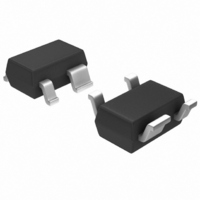
IC AMP MMIC LNA GAAS 3V SOT-343
Manufacturer
Avago Technologies US Inc.
Type
General Purpose Amplifierr
Datasheet
1.MGA-71543-BLKG.pdf
(24 pages)
Specifications of MGA-71543-BLKG
P1db
13.1dBm
Noise Figure
1.1dB ~ 1.45dB
Package / Case
SC-70-4, SC-82-4, SOT-323-4, SOT-343
Current - Supply
50mA ~ 60mA
Frequency
100MHz ~ 6GHz
Gain
14.4dB ~ 17.4dB
Rf Type
CDMA, TDMA, W-CDMA
Test Frequency
2.01GHz
Voltage - Supply
2.7V ~ 4.2V
Mounting Style
SMD/SMT
Technology
Low Noise Amplifier
Number Of Channels
1
Operating Frequency
6000 MHz
Operating Supply Voltage
3 V
Supply Current
50 mA
Maximum Power Dissipation
200 mW
Maximum Operating Temperature
+ 150 C
Manufacturer's Type
Low Noise Amplifier
Frequency (max)
6GHz
Operating Supply Voltage (min)
2.7V
Operating Supply Voltage (typ)
3V
Operating Supply Voltage (max)
4.2V
Package Type
SOT-343
Mounting
Surface Mount
Pin Count
3 +Tab
Noise Figure (typ)
1.1@6000MHzdB
Lead Free Status / RoHS Status
Lead free / RoHS Compliant
Lead Free Status / RoHS Status
Lead free / RoHS Compliant, Lead free / RoHS Compliant
Other names
516-1952
MGA-71543-BLKG
MGA-71543-BLKG
Available stocks
Company
Part Number
Manufacturer
Quantity
Price
Company:

Part Number:
MGA-71543-BLKG
Manufacturer:
NXP
Quantity:
12 000
Part Number:
MGA-71543-BLKG
Manufacturer:
AVAGO/安华高
Quantity:
20 000


14
Designing with MGA-71543,
a Low Noise Amplifier with
Built-in Mitigated Bypass
Switches
Introduction
The MGA-71543 is a single stage
GaAs RFIC low noise amplifier
with an integrated bypass switch
(Figure 1).
Figure 1. MGA-71543 Functional Diagram.
This application note describes a
low noise amplifier design using
Avago Technologies’ MGA-71543.
The MGA-71543 is designed for
receivers and transmitters operat-
ing from 100 MHz to 6 GHz, mainly
for CDMA applications i.e. IS-95
CDMA1900, CDMA800 and
W-CDMA. It can be used as a first
stage (Q1) in a CDMA PCS
1900 MHz application currently
filled by a single transistor. Its
bypass capability adds features
over the single transistor solution
with no performance loss. The
device can also be used as a driver
amplifier for CDMA800.
The purpose of the switch feature
is to prevent distortion of high
signal levels in receiver applica-
tions by bypassing the amplifier.
Furthermore, zero current draw,
when in bypass mode, saves
current thus improving battery
life.
The internally matched switching
circuit provides a 20 dB gain step
and also reduces gain ripple and
mismatch in system usage.
RF IN
Switch & Bias
RF OUT
The MGA-71543 is a small LNA/
Bypass Switch MMIC that pro-
vides a low noise figure, a high
gain and high third order input
intercept point (IIP3) ideal for the
first stage LNA of PCS CDMA and
W-CDMA.
Device Description
The MGA-71543 is a single stage
GaAs IC with a built-in bypass
switch housed in a SOT-343
package. The device diagram is
shown in Figures 1 and 2.
Figure 2. Simplified Schematic.
Figure 3. Bypass State Duplicates the In and
Out Impedance.
The MGA-71543 features a mini-
mum noise figure of 0.8 dB and
16 dB available gain. The input
and output are partially matched,
and only a simple series/shunt
inductor match is required to
achieve low noise figure and
VSWR into 50Ω.
When set into the bypass mode,
both input and output are inter-
nally matched through a mitigative
circuit. This circuit draws no
current (less than 2 µA), yet
duplicates the in and out imped-
ance of the LNA (Figure 3). This
allows the system user to have
minimum mismatch change from
LNA to Bypass mode, thus allow-
Input
DC
RF in
GND
&
ref
Amplifier Mode
Bypass Mode
+
–
Gain FET
Control
+
–
RF out
Output
& V
GND
& Vc
d
ing the same matching network at
both states (LNA State and Bypass
State). This makes the MGA-71543
ideal for use between duplexers
and image reject filters.
The MGA-71543 offers an inte-
grated solution of LNA with
adjustable IIP3. The IIP3 can be
fixed to a desired current level for
the receiver’s linearity require-
ments. The LNA has a bypass
switch function, which sets the
current to zero (2 µA) and pro-
vides low insertion loss when in
bypass mode. The bypass mode
also boosts dynamic range when
high level signal is being received.
Many CDMA systems operate
20% LNA and 80% bypass mode.
For example, with the bypass
draw of zero and LNA of 10 mA,
the MGA-71543 allows an average
of only 2 mA current.
The MGA-71543 is a GaAs MMIC,
processed on Avago’s cost effec-
tive PHEMT (Pseudomorphic High
Electron Mobility Transistor
Technology). It is housed in the
SOT343 (SC70 4-lead) package.
Biasing
This IC can be biased like a
depletion mode discrete GaAsFET.
Two kinds of passive biasing can
be used: gate bias (Figure 4) and
source resistor bias method
(Figure 6).
Gate Bias
Pins 1 and 4 (Figure 4) are DC
grounded and a negative bias
voltage is applied to Pin 3 in
addition to the power supply (2.7
or 3 V) applied to Pin 2. This
method of biasing has the advan-
tage of minimizing parasitic
source inductance because the
device is directly DC and RF
grounded.
Related parts for MGA-71543-BLKG
Image
Part Number
Description
Manufacturer
Datasheet
Request
R

Part Number:
Description:
Amplifier IC
Manufacturer:
Avago Technologies US Inc.
Datasheet:

Part Number:
Description:
IC AMP MMIC LNA GAAS 3V SOT-343
Manufacturer:
Avago Technologies US Inc.
Datasheet:

Part Number:
Description:
AMPLIFIER RFIC GAAS, LOW NOISE
Manufacturer:
Avago Technologies US Inc.
Part Number:
Description:
IC,Microwave/Millimeter Wave Amplifier,SINGLE,GAAS,SOT-343R,PLASTIC
Manufacturer:
Avago Technologies US Inc.
Part Number:
Description:
IC,Microwave/Millimeter Wave Amplifier,SINGLE,GAAS,SOT-343R,PLASTIC
Manufacturer:
Avago Technologies US Inc.
Datasheet:

Part Number:
Description:
OPTOCOUPLER GATE DRV 2A 16-SOIC
Manufacturer:
Avago Technologies US Inc.
Datasheet:
Part Number:
Description:
OPTOCOUPLER 2CH 2.5A 16-SOIC
Manufacturer:
Avago Technologies US Inc.
Datasheet:

Part Number:
Description:
OPTOCOUPLER GATE DRV 0.4A 16SOIC
Manufacturer:
Avago Technologies US Inc.
Datasheet:

Part Number:
Description:
OPTOCOUPLER 2.0A 250KHZ 8-DIP
Manufacturer:
Avago Technologies US Inc.
Datasheet:

Part Number:
Description:
OPTOCOUPLER 2.0A 250KHZ GW 8-SMD
Manufacturer:
Avago Technologies US Inc.
Datasheet:

Part Number:
Description:
OPTOCOUPLER 2CH 15MBD 3.3V 8SOIC
Manufacturer:
Avago Technologies US Inc.
Datasheet:
Part Number:
Description:
OPTOCOUPLER DARL-OUT 8-DIP
Manufacturer:
Avago Technologies US Inc.
Datasheet:
Part Number:
Description:
OPTOCOUPLER IGBT DRIVE 0.4A 8DIP
Manufacturer:
Avago Technologies US Inc.
Datasheet:
Part Number:
Description:
OPTOCOUPLER DARL-OUT 8-DIP
Manufacturer:
Avago Technologies US Inc.
Datasheet:

Part Number:
Description:
OPTOCOUPLER 1CH 1MBS 8-SMD GW
Manufacturer:
Avago Technologies US Inc.
Datasheet: