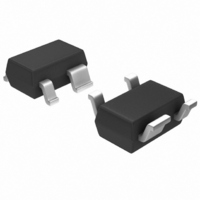
MGA-71543-BLKG Avago Technologies US Inc., MGA-71543-BLKG Datasheet - Page 16

MGA-71543-BLKG
Manufacturer Part Number
MGA-71543-BLKG
Description
IC AMP MMIC LNA GAAS 3V SOT-343
Manufacturer
Avago Technologies US Inc.
Type
General Purpose Amplifierr
Datasheet
1.MGA-71543-BLKG.pdf
(24 pages)
Specifications of MGA-71543-BLKG
P1db
13.1dBm
Noise Figure
1.1dB ~ 1.45dB
Package / Case
SC-70-4, SC-82-4, SOT-323-4, SOT-343
Current - Supply
50mA ~ 60mA
Frequency
100MHz ~ 6GHz
Gain
14.4dB ~ 17.4dB
Rf Type
CDMA, TDMA, W-CDMA
Test Frequency
2.01GHz
Voltage - Supply
2.7V ~ 4.2V
Mounting Style
SMD/SMT
Technology
Low Noise Amplifier
Number Of Channels
1
Operating Frequency
6000 MHz
Operating Supply Voltage
3 V
Supply Current
50 mA
Maximum Power Dissipation
200 mW
Maximum Operating Temperature
+ 150 C
Manufacturer's Type
Low Noise Amplifier
Frequency (max)
6GHz
Operating Supply Voltage (min)
2.7V
Operating Supply Voltage (typ)
3V
Operating Supply Voltage (max)
4.2V
Package Type
SOT-343
Mounting
Surface Mount
Pin Count
3 +Tab
Noise Figure (typ)
1.1@6000MHzdB
Lead Free Status / RoHS Status
Lead free / RoHS Compliant
Lead Free Status / RoHS Status
Lead free / RoHS Compliant, Lead free / RoHS Compliant
Other names
516-1952
MGA-71543-BLKG
MGA-71543-BLKG
Available stocks
Company
Part Number
Manufacturer
Quantity
Price
Company:
Part Number:
MGA-71543-BLKG
Manufacturer:
NXP
Quantity:
12 000
Part Number:
MGA-71543-BLKG
Manufacturer:
AVAGO/安华高
Quantity:
20 000
16
Applying the Device Voltage
Common to all methods of
biasing, voltage V
the MGA-71543 through the RF
output connection (Pin 2). The
bias line is capacitively bypassed
to keep RF from the DC supply
lines and prevent resonant dips or
peaks in the response of the
amplifier. Where practical, it may
be cost effective to use a length of
high impedance transmission line
(usually λ /
RFC.
When using the gate bias method,
the applied device voltage, V
equal to voltage V
V
Figure 9. DC Schematic for Gate Bias.
For source resistor biasing
method, the applied device
voltage, V
control voltage is V
is set by the external bias resistor.
A source resistor bias circuit is
shown in Figure 10.
Input
Figure 10. DC Schematic for Source Bias.
Input
RF
RF
s
is zero.
Vref = -0.5 V
3
3
1
1
71
ds
71
4
, is V
line) in place of the
4
4
R
2
2
bias
d
d
d
– V
is applied to
(at pin 2) since
s
(Pin 4) which
s
. The bias
V
V
d
d
ds
Output
Output
~ +2.5 V
= +3 V
RF
RF
, is
Controlling the Switch
The device current controls the
state of the MGA-71543 (amplifier
or bypass mode). For device
currents greater than 3 mA, it
functions as an amplifier. If a
lower current is drawn, the gain of
the amplifier is significantly
reduced and the performance will
degrade. If the device current is
set to zero, the MGA-71543 is
switched into a bypass mode in
which the signal is routed around
the amplifier with a loss of about
5.6 dB.
The simplest way of switching the
MGA-71543 to the bypass mode is
to open-circuit the terminals at
Pins 1 and 4. The bypass mode is
also set by increasing the source
resistance R
1 MΩ. With the DC ground con-
nection open, the internal control
circuit of the MGA-71543 auto-
switches from amplifier mode into
a bypass mode and the device
current drops to near zero. Typical
bypass mode current is 2 µA.
Figure 11. MGA-71543 Amplifier/Bypass State
Switching.
A digital switch can be used to
control the amplifier and Bypass
State as shown in Figure 11.
Switching Speed
The speed at which the
MGA-71543 switches between
states is extremely fast. The
intrinsic switching speed is
typically around 10 ns. However in
practical circuits, the switching
speed is limited by the time
3
1
bias
R
to greater than
bias
4
2
Bypass Switch
Enable
constants of the external bias
circuit components (current
setting resistor and bypass
capacitors). These external
components increase the switch-
ing time to around 100ns. Further-
more, the switching ON time is
slightly lower (faster) than the
switching OFF time (i.e. It
switches on faster).
Thermal issues
The Mean Time To Failure (MTTF)
of semiconductors is inversely
proportional to the operating
temperature.
When biased at 3V and 10 mA for
LNA applications, the power
dissipation is 3V x 10 mA = 30 mW.
The temperature increment from
the RFIC channel to its case is
then 30 mW x θ
240°C/watt = 7.2°C. Subtracting
the channel-to-case temperature
rise from the suggested maximum
junction temperature of 150°C, the
resulting maximum allowable case
temperature is 143°C.
The worst case thermal situation
occurs when the MGA-71543 is
operated at its maximum operat-
ing conditions in an effort to
maximize output power or achieve
minimum distortion. A similar
calculation for the maximum
operating bias of 4.2 volts and
50 mA yields a maximum allow-
able case temperature of 100°C.
(i.e. 210 mW x θ
240°C/watt = 50.4°C
150°C – 50.4°C = 100°C.)
This calculation assumes the
worst case of no RF power being
extracted from the device. When
operated in a saturated mode,
both power-added efficiency and
the maximum allowable case
temperature will increase.
Note: “Case” temperature for
surface mount packages such as
the SOT-343 refers to the interface
between the package pins and the
jc
jc
= 0.030 watt x
= 0.210 watt x


