MGA-71543-BLKG Avago Technologies US Inc., MGA-71543-BLKG Datasheet - Page 17
MGA-71543-BLKG
Manufacturer Part Number
MGA-71543-BLKG
Description
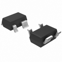
IC AMP MMIC LNA GAAS 3V SOT-343
Manufacturer
Avago Technologies US Inc.
Type
General Purpose Amplifierr
Datasheet
1.MGA-71543-BLKG.pdf
(24 pages)
Specifications of MGA-71543-BLKG
P1db
13.1dBm
Noise Figure
1.1dB ~ 1.45dB
Package / Case
SC-70-4, SC-82-4, SOT-323-4, SOT-343
Current - Supply
50mA ~ 60mA
Frequency
100MHz ~ 6GHz
Gain
14.4dB ~ 17.4dB
Rf Type
CDMA, TDMA, W-CDMA
Test Frequency
2.01GHz
Voltage - Supply
2.7V ~ 4.2V
Mounting Style
SMD/SMT
Technology
Low Noise Amplifier
Number Of Channels
1
Operating Frequency
6000 MHz
Operating Supply Voltage
3 V
Supply Current
50 mA
Maximum Power Dissipation
200 mW
Maximum Operating Temperature
+ 150 C
Manufacturer's Type
Low Noise Amplifier
Frequency (max)
6GHz
Operating Supply Voltage (min)
2.7V
Operating Supply Voltage (typ)
3V
Operating Supply Voltage (max)
4.2V
Package Type
SOT-343
Mounting
Surface Mount
Pin Count
3 +Tab
Noise Figure (typ)
1.1@6000MHzdB
Lead Free Status / RoHS Status
Lead free / RoHS Compliant
Lead Free Status / RoHS Status
Lead free / RoHS Compliant, Lead free / RoHS Compliant
Other names
516-1952
MGA-71543-BLKG
MGA-71543-BLKG
Available stocks
Company
Part Number
Manufacturer
Quantity
Price
Company:

Part Number:
MGA-71543-BLKG
Manufacturer:
NXP
Quantity:
12 000
Part Number:
MGA-71543-BLKG
Manufacturer:
AVAGO/安华高
Quantity:
20 000


17
mounting surface, i.e., the tem-
perature at the PCB mounting
pads. The primary heat path from
the RFIC chip to the system
heatsink is by means of conduc-
tion through the package leads
and ground vias to the ground
plane of the PCB.
Grounding Consideration in
PCB Layout
The MGA-71543 requires careful
attention during grounding. Any
device with gain can be made to
oscillate if feedback is added.
Since poor grounding adds series
feedback, it can cause the device
to oscillate. Poor grounding is one
of the most common causes of
oscillation in RF components.
Careful attention should be used
when RF bypassing the ground
terminals when the device is
biased using the source resistor
method.
Package Footprint
The PCB pad print for the minia-
ture, 4-lead SOT-343 (SC70)
package is shown in Figure 12.
0.039
Figure 12. Recommended PCB Pad Layout for
Avago’s SC70 4L/SOT-343 Products.
The layout is shown with a
footprint of the MGA-71543
superimposed on the PCB pads for
reference.
1.00
0.024
0.60
0.045
1.15
0.051
1.30
Dimensions in mm
inches
0.079
2.00
0.035
0.9
RF bypass
For layouts using the source
resistor method of biasing, both of
the ground terminals of the
MGA-71543 must be well bypassed
to maintain device stability.
Beginning with the package pad
print in Figure 12, and RF layout
similar to the one shown in
Figure 13 is a good starting point
for using the MGA-71543 with
capacitor-bypassed ground
terminals. It is a best practice to
use multiple vias to minimize
overall ground path inductance.
Figure 13. Layout for RF Bypass.
PCB Materials
0.031 inches thick of FR-4 or G-10
type dielectric materials are
typical choices for most low cost
wireless applications using single
layer printed boards. As an
alternative, a Getek material with
a multilayer printed circuit board
can be used for a smaller size
board, where:
1
2
3
4
The spacing between the layers is
as follows:
Between the 1
Between the 2
Between the 3
Size 0402
recommended
for the bypass
capacitors
st
nd
rd
th
layer: RF routing layer
layer: Other RF routing layer
layer: Power (DC) routing layer
layer: Ground layer
71
st
nd
rd
and 2
and 4
and 3
nd
th
rd
: 0.005"
: 0.005"
: 0.020"
LNA Application
In the following sections the LNA
design is described in a more
general way. Sample evaluation
boards for 1900 MHz and 800 MHz
are shown in a table (Table 1) and
the appropriate board diagram is
shown (Figures 22 and 23). A
second smaller size board is also
shown (Figures 25 and 26) with
the corresponding table (Table 2).
The smaller board is an example
of reducing the size of the layout,
more suitable for handset manu-
facturers. For low noise amplifier
application, the LNA is typically
biased 6 to 20 mA.
The MGA-71543 is a conditionally
stable device, therefore, the
proper input and output loads
must be presented in addition to
properly RF grounding the device.
Please refer to the stability section
for tips on preventing oscillation.
The LNA can be switched ON or
OFF by a simply varying the
resistor to its ground leads as
described in previous sections.
Matching Networks for the LNA
50Ω
Figure 14. Input and Output Matching
Terminology.
The input matching network
determines the noise figure and
return loss (S11) of our amplifier.
The output-matching network
determines the IP3 and output
return loss (S22). Furthermore,
both input and output matching
networks influence the gain. The
best gain (Maximum Available
Gain-MAG) and lowest input
return loss is obtained when both
the input and output are conju-
Input
Match
Γ
in
Γ
or
Γ
s
opt
LNA
Γ
L
Γ
opt
Output
Match
50Ω
Related parts for MGA-71543-BLKG
Image
Part Number
Description
Manufacturer
Datasheet
Request
R

Part Number:
Description:
Amplifier IC
Manufacturer:
Avago Technologies US Inc.
Datasheet:

Part Number:
Description:
IC AMP MMIC LNA GAAS 3V SOT-343
Manufacturer:
Avago Technologies US Inc.
Datasheet:

Part Number:
Description:
AMPLIFIER RFIC GAAS, LOW NOISE
Manufacturer:
Avago Technologies US Inc.
Part Number:
Description:
IC,Microwave/Millimeter Wave Amplifier,SINGLE,GAAS,SOT-343R,PLASTIC
Manufacturer:
Avago Technologies US Inc.
Part Number:
Description:
IC,Microwave/Millimeter Wave Amplifier,SINGLE,GAAS,SOT-343R,PLASTIC
Manufacturer:
Avago Technologies US Inc.
Datasheet:

Part Number:
Description:
OPTOCOUPLER GATE DRV 2A 16-SOIC
Manufacturer:
Avago Technologies US Inc.
Datasheet:
Part Number:
Description:
OPTOCOUPLER 2CH 2.5A 16-SOIC
Manufacturer:
Avago Technologies US Inc.
Datasheet:

Part Number:
Description:
OPTOCOUPLER GATE DRV 0.4A 16SOIC
Manufacturer:
Avago Technologies US Inc.
Datasheet:

Part Number:
Description:
OPTOCOUPLER 2.0A 250KHZ 8-DIP
Manufacturer:
Avago Technologies US Inc.
Datasheet:

Part Number:
Description:
OPTOCOUPLER 2.0A 250KHZ GW 8-SMD
Manufacturer:
Avago Technologies US Inc.
Datasheet:

Part Number:
Description:
OPTOCOUPLER 2CH 15MBD 3.3V 8SOIC
Manufacturer:
Avago Technologies US Inc.
Datasheet:
Part Number:
Description:
OPTOCOUPLER DARL-OUT 8-DIP
Manufacturer:
Avago Technologies US Inc.
Datasheet:
Part Number:
Description:
OPTOCOUPLER IGBT DRIVE 0.4A 8DIP
Manufacturer:
Avago Technologies US Inc.
Datasheet:
Part Number:
Description:
OPTOCOUPLER DARL-OUT 8-DIP
Manufacturer:
Avago Technologies US Inc.
Datasheet:

Part Number:
Description:
OPTOCOUPLER 1CH 1MBS 8-SMD GW
Manufacturer:
Avago Technologies US Inc.
Datasheet: