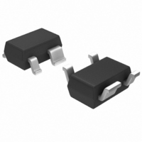
MGA-71543-BLKG Avago Technologies US Inc., MGA-71543-BLKG Datasheet - Page 4

MGA-71543-BLKG
Manufacturer Part Number
MGA-71543-BLKG
Description
IC AMP MMIC LNA GAAS 3V SOT-343
Manufacturer
Avago Technologies US Inc.
Type
General Purpose Amplifierr
Datasheet
1.MGA-71543-BLKG.pdf
(24 pages)
Specifications of MGA-71543-BLKG
P1db
13.1dBm
Noise Figure
1.1dB ~ 1.45dB
Package / Case
SC-70-4, SC-82-4, SOT-323-4, SOT-343
Current - Supply
50mA ~ 60mA
Frequency
100MHz ~ 6GHz
Gain
14.4dB ~ 17.4dB
Rf Type
CDMA, TDMA, W-CDMA
Test Frequency
2.01GHz
Voltage - Supply
2.7V ~ 4.2V
Mounting Style
SMD/SMT
Technology
Low Noise Amplifier
Number Of Channels
1
Operating Frequency
6000 MHz
Operating Supply Voltage
3 V
Supply Current
50 mA
Maximum Power Dissipation
200 mW
Maximum Operating Temperature
+ 150 C
Manufacturer's Type
Low Noise Amplifier
Frequency (max)
6GHz
Operating Supply Voltage (min)
2.7V
Operating Supply Voltage (typ)
3V
Operating Supply Voltage (max)
4.2V
Package Type
SOT-343
Mounting
Surface Mount
Pin Count
3 +Tab
Noise Figure (typ)
1.1@6000MHzdB
Lead Free Status / RoHS Status
Lead free / RoHS Compliant
Lead Free Status / RoHS Status
Lead free / RoHS Compliant, Lead free / RoHS Compliant
Other names
516-1952
MGA-71543-BLKG
MGA-71543-BLKG
Available stocks
Company
Part Number
Manufacturer
Quantity
Price
Company:
Part Number:
MGA-71543-BLKG
Manufacturer:
NXP
Quantity:
12 000
Part Number:
MGA-71543-BLKG
Manufacturer:
AVAGO/安华高
Quantity:
20 000
4
MGA-71543 Typical Performance
T
and was optimized for each frequency with external tuners.
Figure 4. MGA-71543 Production Test Circuit.
Input
V
RF
c
ref
Figure 9. Associated Gain with Fmin vs.
Frequency.
Figure 12. S22 Impedance vs. Frequency.
(m1 = Sw, m2 = 6 mA, m3 = 10 mA)
Figure 6. Minimum Noise Figure vs.
Frequency and Voltage.
2.7 nH
1.5
1.3
1.1
0.9
0.7
0.5
14
= 25°C, Z
20
17
11
8
5
0
0
56 pF
1.5 nH
1
1
o
500 MHz to 6 GHz
= 50, V
FREQUENCY (GHz)
FREQUENCY (GHz)
2
2
3
4
3
3
d
m3
= 3V, I
4
4
m2 m1
2
1
d
= 10 mA unless stated otherwise. Data vs. frequency was measured in Figure 5 test system
5
5
-40°C
+25°C
+85°C
2.7V
3.0V
3.3V
6
6
3.9 nH
960 pF
56 pF
Figure 13. Bypass Mode Associated
Insertion Loss with Fmin Match and
Minimum Loss vs. Frequency.
56 pF
Figure 7. Associated Gain with Fmin vs.
Frequency and Voltage.
Figure 10. Input Third Order Intercept Point
vs. Frequency and Temperature.
-10
20
17
14
11
18
15
12
-3
-2
-4
-6
-8
8
5
9
6
3
0
0
0
0
0
Output
V
RF
ds
1
1
1
FREQUENCY (GHz)
FREQUENCY (GHz)
FREQUENCY (GHz)
2
2
2
3
3
3
Figure 5. MGA-71543 Test Circuit for S, Noise, and
Power Parameters over Frequency.
Input Bias Tee
V
RF
ref
4
4
4
G
Minimum
ass
5
5
5
-40°C
+25°C
+85°C
w/Fmin
2.7V
3.0V
3.3V
6
6
6
Test Fixture
Figure 14. Output Power at 1 dB Compression
vs. Frequency and Voltage.
Figure 8. Input Third Order Intercept Point vs.
Frequency and Voltage.
Figure 11. S11 Impedance vs. Frequency.
(m1 = Sw, m2 = 6 mA, m3 = 10 mA)
18
15
12
18
15
12
-3
-3
9
6
3
0
9
6
3
0
m1
0
0
m2
m3
1
1
500 MHz to 6 GHz
FREQUENCY (GHz)
FREQUENCY (GHz)
2
2
Bias
Tee
3
3
[4]
4
4
Output
V
RF
ds
5
5
2.7V
3.0V
3.3V
2.7V
3.0V
3.3V
6
6


