MGA-30689-BLKG Avago Technologies US Inc., MGA-30689-BLKG Datasheet
MGA-30689-BLKG
Specifications of MGA-30689-BLKG
MGA-30689-BLKG


Related parts for MGA-30689-BLKG


MGA-30689-BLKG Summary of contents
Page 1
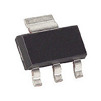
... GaAs Enhancement-mode pHEMT process. The device required simple dc biasing components to achieve wide bandwidth performance. The tempera- ture compensated internal bias circuit provides stable current over temperature and process threshold voltage variation. The MGA-30689 is housed inside a standard SOT89 package (4.5 x 4.1 x 1.5 mm). Component Image 6GX #1 #2 ...
Page 2
Absolute Maximum Rating T =25 °C A Symbol Parameter V Device Voltage, RF output to ground dd,max Input Power in,max P Total Power Dissipation diss T Junction Temperature j, max T Storage Temperature STG Product Consistency ...
Page 3
Electrical Specifications T = 25°C, Vdd =5V A Symbol Parameter and Test Condition Ids Quiescent current Gain Gain [8] OIP3 Output Third Order Intercept Point NF Noise Figure S11 Input Return Loss, 50: source S22 Output Return Loss, 50: ...
Page 4
Typical Performance (40MHz – 2GHz +25°C, Vdd = 5V, Input Signal = CW. Application Test Circuit is shown in Figure 30 and Table 1. 120 110 100 90 80 -40 -30 -20 - ...
Page 5
Typical Performance (40MHz – 2GHz +25°C, Vdd = 5V, Input Signal = CW. Application Test Circuit is shown in Figure 30 and Table -10 -15 -20 -25 -30 0.0 0.2 0.4 0.6 0.8 1.0 1.2 ...
Page 6
Typical Performance (0.2GHz – 3GHz +25°C, Vdd = 5V, Input Signal = CW. Application Test Circuit is shown in Figure 30 and Table 2. 120 110 100 90 80 -40 -30 -20 - ...
Page 7
Typical Performance (0.2GHz – 3GHz +25°C, Vdd = 5V, Input Signal = CW. Application Test Circuit is shown in Figure 30 and Table -10 -15 -20 -25 -30 0.2 0.6 1.0 1.4 1.8 Frequency (GHz) ...
Page 8
Typical Performance (1.5GHz – 2.6GHz +25°C, Vdd = 5V, Input Signal = CW. Application Test Circuit is shown in Figure 30 and Table 3. 120 110 100 90 80 -40 -30 -20 - ...
Page 9
Typical Performance (1.5GHz – 2.6GHz +25°C, Vdd = 5V, Input Signal = CW. Application Test Circuit is shown in Figure 30 and Table -10 -15 -20 -25 -30 1.5 1.6 1.7 1.8 1.9 2.0 2.1 ...
Page 10
Application Schematic Components Table and Demo Board Top View C7 RFin RFin 1 GND Figure 30. Application Schematic – Recommended PCB material is 10 mils Rogers RO4350, with FR4 backing for mechanical strength. – Suggested component values may vary according ...
Page 11
Demo board Part List Table 1. 40 MHz – 2 GHz Application Schematic Components Circuit Symbol Size Value L2 0805 820nH C4 0402 100pF C5 0402 0.1uF C6 0805 2.2uF C7 0402 0.1uF C8 0402 0.1uF Table 2. 0.2 GHz ...
Page 12
Typical S-Parameter (Vdd=5V, T=25°C, 50 ohm) Freq S11 S11 (GHz) (dB) (ang) 0.04 -12.99 -32.00 0.1 -14.08 -27.40 0.2 -14.01 -38.85 0.3 -13.91 -53.66 0.4 -13.77 -68.63 0.5 -13.35 -83.56 0.6 -13.00 -97.71 0.7 -12.72 -111.41 0.8 -12.52 -124.63 0.9 ...
Page 13
... Part Number Ordering Information Part Number No. of Devices MGA-30689-BLKG 100 MGA-30689-TR1G 3000 SOT89 Package Dimensions Y R0.254 TYP. (R0.010" TYP Z 0.10 ...
Page 14
Device Orientation REEL USER FEED COVER TAPE DIRECTION Tape Dimensions 8.00±0.10 Ø1.50±0.10 (0.315±0.004) (0.059±0.004) 12.0±0.30–0.10 (0.472+0.012–0.004) 8° 4.80±0.10 (0.180±0.004) Dimensions in mm (inches) 14 6GX CARRIER TAPE 4.00±0.10 (0.157±0.004) (0.069±0.004) + Ø1.50±0.25 (0.059±0.010) 0.292±0.02 (0.0115±0.0008) 0.180±0.10 (0.0709±0.004) 4.40±0.10 (0.1732±0.004) 6GX ...
Page 15
Reel Dimensions – 13” Reel 12mm width DATE CODE EMBOSSED LETTERING 7.5mm HEIGHT EMBOSSED LINE (2x) 89.0mm LENGTH LINES 147.0mm AWAY FROM CENTER POINT ESD LOGO 6 PS ...