AD8351ARMZ Analog Devices Inc, AD8351ARMZ Datasheet
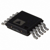
IC DIFF AMP RF/IF LOWDIST 10MSOP

AD8351ARMZ

Manufacturer Part Number
AD8351ARMZ
Description
IC DIFF AMP RF/IF LOWDIST 10MSOP
Manufacturer
Analog Devices Inc
Datasheet

Specifications of AD8351ARMZ

Gain
26dB
Rf Type
General Purpose
Current - Supply
28mA ~ 32mA
Frequency
10MHz ~ 2.5GHz
P1db
13.5dBm
Package / Case
10-MSOP, Micro10™, 10-uMAX, 10-uSOP
Test Frequency
10MHz
Voltage - Supply
3 V ~ 5 V
Frequency Range
2.2GHz
Power Dissipation Pd
320mW
Supply Current
28mA
Supply Voltage Range
3V To 5.5V
Rf Ic Case Style
MSOP
No. Of Pins
10
Number Of Channels
1
Operating Supply Voltage (min)
3V
Operating Supply Voltage (typ)
5V
Operating Supply Voltage (max)
5.5V
Package Type
MSOP
Mounting
Surface Mount
Pin Count
10
Operating Temp Range
-40C to 85C
Operating Temperature Classification
Industrial
Lead Free Status / RoHS Status
Lead free / RoHS Compliant
Noise Figure
-
Lead Free Status / Rohs Status
Compliant

Available stocks

Company
Part Number
Manufacturer
Quantity
Price
Part Number:
AD8351ARMZ
Manufacturer:
AD
Quantity:
106
Part Number:
AD8351ARMZ
Manufacturer:
AnalogDevice
Quantity:
115
Part Number:
AD8351ARMZ
Manufacturer:
ADI/亚德诺
Quantity:
20 000
Part Number:
AD8351ARMZ-REEL
Manufacturer:
LT
Quantity:
776
Part Number:
AD8351ARMZ-REEL7
Manufacturer:
ADI/亚德诺
Quantity:
20 000
GENERAL DESCRIPTION
The AD8351 is a low cost differential amplifier useful in RF and
IF applications up to 2.2 GHz. The voltage gain can be set from
unity to 26 dB using a single external gain resistor. The AD8351
provides a nominal 150 Ω differential output impedance. The
excellent distortion performance and low noise characteristics of
this device allow for a wide range of applications.
The AD8351 is designed to satisfy the demanding performance
requirements of communications transceiver applications. The
device can be used as a general-purpose gain block, an ADC driver,
REV. B
Information furnished by Analog Devices is believed to be accurate and
reliable. However, no responsibility is assumed by Analog Devices for its
use, nor for any infringements of patents or other rights of third parties that
may result from its use. No license is granted by implication or otherwise
under any patent or patent rights of Analog Devices. Trademarks and
registered trademarks are the property of their respective owners.
FEATURES
–3 dB Bandwidth of 2.2 GHz for A
Single Resistor Programmable Gain
Differential Interface
Low Noise Input Stage 2.7 nV/√Hz @ A
Low Harmonic Distortion
–79 dBc Second @ 70 MHz
–81 dBc Third @ 70 MHz
OIP3 of 31 dBm @ 70 MHz
Single-Supply Operation: 3 V to 5.5 V
Low Power Dissipation: 28 mA @ 5 V
Adjustable Output Common-Mode Voltage
Fast Settling and Overdrive Recovery
Slew Rate of 13,000 V/ s
Power-Down Capability
10-Lead MSOP Package
APPLICATIONS
Differential ADC Drivers
Single-Ended-to-Differential Conversion
IF Sampling Receivers
RF/IF Gain Blocks
SAW Filter Interfacing
0 dB ≤ A
V
≤ 26 dB
V
= 12 dB
V
= 10 dB
and a high speed data interface driver, among other functions. The
AD8351 can also be used as a single-ended-to-differential
amplifier with similar distortion products as in the differential
configuration. The exceptionally good distortion performance
makes the AD8351 an ideal solution for 12-bit and 14-bit IF
sampling receiver designs.
Fabricated in ADI’s high speed XFCB process, the AD8351
has high bandwidth that provides high frequency performance
and low distortion. The quiescent current of the AD8351 is 28 mA
typically. The AD8351 amplifier comes in a compact 10-lead
MSOP package and will operate over the temperature range
of –40°C to +85°C.
One Technology Way, P.O. Box 9106, Norwood, MA 02062-9106, U.S.A.
Tel: 781/329-4700
Fax: 781/326-8703
–100
–110
–120
–130
–10
–20
–30
–40
–50
–60
–70
–80
–90
0
0
AD8351 WITH 10 dB OF
GAIN DRIVING THE
AD6645 (R L = 1k )
ANALOG INPUT: 70MHz
ENCODE : 80MHz
SNR :
FUND : –1.1dBFS
HD2 :
HD3 :
THD :
SFDR : 78.2dBc
Differential RF/IF Amplifier
PWUP
5
RGP1
RGP2
INLO
INHI
FUNCTIONAL BLOCK DIAGRAM
–78.5dBc
–80.7dBc
–75.9dBc
69.1dB
+
AD8351
10
© 2004 Analog Devices, Inc. All rights reserved.
15
INLO
INHI
200
BIAS CELL
RG
20
Low Distortion
AD8351
AD8351
25
100nF 25
100nF
AD8351
2
25
VOCM
VPOS
OPHI
OPLO
COMM
www.analog.com
30
14-BIT ADC
AD6645
35
3

Related parts for AD8351ARMZ

AD8351ARMZ Summary of contents

Page 1

FEATURES –3 dB Bandwidth of 2.2 GHz for A Single Resistor Programmable Gain 0 dB ≤ A ≤ Differential Interface Low Noise Input Stage 2.7 nV/√ Low Harmonic Distortion –79 dBc Second @ 70 MHz ...

Page 2

AD8351–SPECIFICATIONS Parameter Conditions DYNAMIC PERFORMANCE –3 dB Bandwidth GAIN = 6 dB, V GAIN = 12 dB, V GAIN = 18 dB ≤ GAIN ≤ 20 dB, V Bandwidth for 0.1 dB Flatness 0 dB ≤ GAIN ...

Page 3

Parameter Conditions NOISE/DISTORTION 10 MHz Second/Third Harmonic 2 Distortion Third-Order IMD OUT OUT Output Third-Order Intercept f1 = 9.5 MHz 10.5 MHz Noise Spectral Density (RTI ...

Page 4

AD8351 ABSOLUTE MAXIMUM RATINGS* Supply Voltage VPOS . . . . . . . . . . . . . . . . . . . . . . . . . . . . . 6 V PWUP Voltage ...

Page 5

unless otherwise noted 200 – 100 FREQUENCY (MHz) TPC 1. Gain vs. Frequency ...

Page 6

AD8351 –30 HD3 –40 HD2 –50 –60 –70 –80 DIFFERENTIAL INPUT –90 –100 100 125 150 FREQUENCY (MHz) TPC 7. Harmonic Distortion vs. Frequency for Ω (A into R = ...

Page 7

R = 150 L 12 VPOS = 150 L VPOS = 100 125 150 FREQUENCY (MHz) ...

Page 8

AD8351 4000 3500 3000 2500 2000 1500 1000 500 0 10 100 FREQUENCY (MHz) TPC 19. Input Impedance vs. Frequency 160 150 140 130 120 110 100 0 100 FREQUENCY (MHz) TPC 20. Output Impedance vs. Frequency 0 –2 –4 ...

Page 9

TIME (ns) TPC 25. Transient Response under Capacitive = 150 Ω Loading ( pF, 2 pF, 5 pF, 10 pF) ...

Page 10

AD8351 BASIC CONCEPTS Differential signaling is used in high performance signal chains, where distortion performance, signal-to-noise ratio, and low power consumption is critical. Differential circuits inherently provide improved common-mode rejection and harmonic distortion perfor- mance as well as better immunity ...

Page 11

SERIES Figure 4. Smith Chart Representation of SAW Filter Output Matching Network 0 AD8351 50 0 Figure 5. Single-Ended Application SINGLE-ENDED-TO-DIFFERENTIAL OPERATION The AD8351 can ...

Page 12

AD8351 R F INHI OPHI R1 100nF SINGLE- 50 ENDED R AD8351 G 50 SOURCE OPLO INLO VOCM 25 100nF Figure 8. ADC Driving Application Using Single-Ended Input ANALOG MULTIPLEXING The AD8351 can be used as an analog multiplexer in ...

Page 13

It is important to ensure that all I/O, ground, and R be kept as short as possible. In addition required that the ground plane be removed from under the package. Due to the inverse relationship between the gain ...

Page 14

AD8351 EVALUATION BOARD An evaluation board is available for experimentation. Various parameters such as gain, common-mode level, and input and output network configurations can be modified through minor resistor changes. The schematic and evaluation board artwork are presented in Figures ...

Page 15

Component Function P1-1, P1-2, Supply and Ground Pins. VPOS, AGND P1-3 Common-Mode Offset Pin. Allows for monitoring or adjustment of the output common-mode voltage. W1, R7, P1-4, R17, R18 Device Enable. Configured such that switch W1 disables the device when ...

Page 16

AD8351 3.00 BSC 3.00 BSC 0.95 0.85 0.75 Revision History Location 2/04—Data Sheet changed from REV REV. B. Changes to ORDERING GUIDE . . . . . . . . . . . . . . . . ...

Related keywords