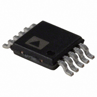
AD8351ARMZ Analog Devices Inc, AD8351ARMZ Datasheet - Page 12

AD8351ARMZ
Manufacturer Part Number
AD8351ARMZ
Description
IC DIFF AMP RF/IF LOWDIST 10MSOP
Manufacturer
Analog Devices Inc
Datasheet
1.AD8351ARMZ.pdf
(16 pages)
Specifications of AD8351ARMZ
Gain
26dB
Rf Type
General Purpose
Current - Supply
28mA ~ 32mA
Frequency
10MHz ~ 2.5GHz
P1db
13.5dBm
Package / Case
10-MSOP, Micro10™, 10-uMAX, 10-uSOP
Test Frequency
10MHz
Voltage - Supply
3 V ~ 5 V
Frequency Range
2.2GHz
Power Dissipation Pd
320mW
Supply Current
28mA
Supply Voltage Range
3V To 5.5V
Rf Ic Case Style
MSOP
No. Of Pins
10
Number Of Channels
1
Operating Supply Voltage (min)
3V
Operating Supply Voltage (typ)
5V
Operating Supply Voltage (max)
5.5V
Package Type
MSOP
Mounting
Surface Mount
Pin Count
10
Operating Temp Range
-40C to 85C
Operating Temperature Classification
Industrial
Lead Free Status / RoHS Status
Lead free / RoHS Compliant
Noise Figure
-
Lead Free Status / Rohs Status
Compliant
Available stocks
Company
Part Number
Manufacturer
Quantity
Price
Company:
Part Number:
AD8351ARMZ
Manufacturer:
AD
Quantity:
106
Company:
Part Number:
AD8351ARMZ
Manufacturer:
AnalogDevice
Quantity:
115
Part Number:
AD8351ARMZ
Manufacturer:
ADI/亚德诺
Quantity:
20 000
Company:
Part Number:
AD8351ARMZ-REEL
Manufacturer:
LT
Quantity:
776
Part Number:
AD8351ARMZ-REEL7
Manufacturer:
ADI/亚德诺
Quantity:
20 000
AD8351
ANALOG MULTIPLEXING
The AD8351 can be used as an analog multiplexer in applications
where it is desirable to select multiple high speed signals. The
isolation of each device when in a disabled state (PWUP pin pulled
low) is about 60 dBc for the maximum input level of 0.5 V p-p out
to 100 MHz. The low output noise spectral density allows for a
simple implementation as depicted in Figure 9. The PWUP inter-
face can be easily driven using most standard logic interfaces. By
using an N-bit digital interface, up to N devices can be controlled.
Output loading effects and noise need to be considered when using
a large number of input signal paths. Each disabled AD8351 pre-
sents approximately a 700 Ω load in parallel with the 150 Ω output
source impedance of the enabled device. As the load increases due
to the addition of N devices, the distortion performance will degrade
due to the heavier loading. Distortion better than –70 dBc can be
achieved with four devices muxed into a 1 kΩ load for signal fre-
quencies up to 70 MHz.
Figure 8. ADC Driving Application Using Single-Ended Input
SOURCE
SINGLE-
ENDED
50
Figure 9. Using Several AD8351s to Form an
N-Channel Analog MUX
INPUT N
INPUT 1
INPUT 2
SIGNAL
SIGNAL
SIGNAL
R1
50
25
R
R
R
G
G
G
100nF
100nF
RGP1
RGP2
RGP1
RGP2
RGP1
RGP2
INLO
INLO
INLO
R
INHI
INHI
INHI
INLO
G
INHI
AD8351
AD8351
AD8351
R
AD8351
F
PWUP
PWUP
PWUP
BIT N
BIT 1
BIT 2
OPHI
OPLO
OPHI
OPLO
OPHI
OPLO
VOCM
OPHI
OPLO
25
25
100nF
N-BIT
DIGITAL
INTERFACE
AIN
AIN VREF
AD6645
MUX
OUTPUT
LOAD
DIGITAL
OUT
–12–
I/O CAPACITIVE LOADING
Input or output direct capacitive loading greater than a few pico-
farads can result in excessive peaking and/or oscillation outside
the pass band. This results from the package and bond wire induc-
tance resonating in parallel with the input/output capacitance of
the device and the associated coupling that results internally
through the ground inductance. For low resistive load or source
resistance, the effective Q is lower, and higher relative capaci-
tance termination(s) can be allowed before oscillation or excessive
peaking occurs. These effects can be eliminated by adding series
input resistors (R
resistors (R
25 Ω is all that is required for I/O capacitive loading greater than
~2 pF. The higher the C, the smaller the R parasitic suppression
resistor required. In addition, R
in-band peaking, especially for light resistive loads.
Due to package parasitic capacitance on the R
values (low gain) cause high ac-peaking inside the pass band,
resulting in poor settling in the time domain. As an example,
when driving a 1 kΩ load, using 25 Ω for R
by ~7 dB for R
C
C
STRAY
STRAY
Figure 10. Input and Output Parasitic Suppression
Resistors, R
Capacitive Loading Effects
Figure 11. Reducing Gain Peaking with Parasitic
Suppressing Resistors (R
OP
) for high load capacitance. Generally less than
G
equal to 200 Ω (A
IP
R
R
) for high source capacitance, or series output
R
IP
IP
IP
G
and R
AD8351
OP
, Used to Suppress
IP
also helps to reduce low gain
IP
V
= 10 dB) (see Figure 11).
= 25 Ω , R
R
R
OP
OP
IP
reduces the peaking
L
G
= 1 k Ω )
ports, high R
C
C
L
L
REV. B
1k
R
L
G


