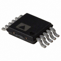
AD8351ARMZ Analog Devices Inc, AD8351ARMZ Datasheet - Page 4

AD8351ARMZ
Manufacturer Part Number
AD8351ARMZ
Description
IC DIFF AMP RF/IF LOWDIST 10MSOP
Manufacturer
Analog Devices Inc
Datasheet
1.AD8351ARMZ.pdf
(16 pages)
Specifications of AD8351ARMZ
Gain
26dB
Rf Type
General Purpose
Current - Supply
28mA ~ 32mA
Frequency
10MHz ~ 2.5GHz
P1db
13.5dBm
Package / Case
10-MSOP, Micro10™, 10-uMAX, 10-uSOP
Test Frequency
10MHz
Voltage - Supply
3 V ~ 5 V
Frequency Range
2.2GHz
Power Dissipation Pd
320mW
Supply Current
28mA
Supply Voltage Range
3V To 5.5V
Rf Ic Case Style
MSOP
No. Of Pins
10
Number Of Channels
1
Operating Supply Voltage (min)
3V
Operating Supply Voltage (typ)
5V
Operating Supply Voltage (max)
5.5V
Package Type
MSOP
Mounting
Surface Mount
Pin Count
10
Operating Temp Range
-40C to 85C
Operating Temperature Classification
Industrial
Lead Free Status / RoHS Status
Lead free / RoHS Compliant
Noise Figure
-
Lead Free Status / Rohs Status
Compliant
Available stocks
Company
Part Number
Manufacturer
Quantity
Price
Company:
Part Number:
AD8351ARMZ
Manufacturer:
AD
Quantity:
106
Company:
Part Number:
AD8351ARMZ
Manufacturer:
AnalogDevice
Quantity:
115
Part Number:
AD8351ARMZ
Manufacturer:
ADI/亚德诺
Quantity:
20 000
Company:
Part Number:
AD8351ARMZ-REEL
Manufacturer:
LT
Quantity:
776
Part Number:
AD8351ARMZ-REEL7
Manufacturer:
ADI/亚德诺
Quantity:
20 000
AD8351
ABSOLUTE MAXIMUM RATINGS*
Supply Voltage VPOS . . . . . . . . . . . . . . . . . . . . . . . . . . . . . 6 V
PWUP Voltage . . . . . . . . . . . . . . . . . . . . . . . . . . . . . . . VPOS
Internal Power Dissipation . . . . . . . . . . . . . . . . . . . . . 320 mW
Maximum Junction Temperature . . . . . . . . . . . . . . . . . 125°C
Operating Temperature Range . . . . . . . . . . . . –40°C to +85°C
Storage Temperature Range . . . . . . . . . . . . . –65°C to +150°C
Lead Temperature Range (Soldering 60 sec) . . . . . . . . . 300°C
*Stresses above those listed under Absolute Maximum Ratings may cause perma-
Model
AD8351ARM
AD8351ARM-R2
AD8351ARM-REEL7
AD8351-EVAL
Pin No.
1
2
3
4
5
6
7
8
9
10
CAUTION
ESD (electrostatic discharge) sensitive device. Electrostatic charges as high as 4000 V readily
accumulate on the human body and test equipment and can discharge without detection. Although the
AD8351 features proprietary ESD protection circuitry, permanent damage may occur on devices
subjected to high energy electrostatic discharges. Therefore, proper ESD precautions are recommended
to avoid performance degradation or loss of functionality.
nent damage to the device. This is a stress rating only; functional operation of the
device at these or any other conditions above those indicated in the operational
section of this specification is not implied. Exposure to absolute maximum rating
conditions for extended periods may affect device reliability.
JA
. . . . . . . . . . . . . . . . . . . . . . . . . . . . . . . . . . . . . . . 125°C/W
Name
PWUP
RGP1
INHI
INLO
RGP2
COMM
OPLO
OPHI
VPOS
VOCM
Temp. Range
–40°C to +85°C
–40°C to +85°C
–40°C to +85°C
Function
Apply a positive voltage (1.3 V ≤ V
Gain Resistor Input 1.
Balanced Differential Input. Biased to midsupply, typically ac-coupled
Balanced Differential Input. Biased to midsupply, typically ac-coupled.
Gain Resistor Input 2.
Device Common. Connect to low impedance ground.
Balanced Differential Output. Biased to VOCM, typically ac-coupled.
Balanced Differential Output. Biased to VOCM, typically ac-coupled.
Positive Supply Voltage. 3 V to 5.5 V.
Voltage applied to this pin sets the common-mode voltage at both the input and output.
Typically decoupled to ground with a 0.1 µF capacitor.
PIN FUNCTION DESCRIPTIONS
Package Description
10-Lead MSOP, 7" Tape and Reel
10-Lead MSOP, 7" Tape and Reel
10-Lead MSOP, 7" Tape and Reel
Evaluation Board
ORDERING GUIDE
–4–
PWUP
≤ VPOS ) to activate device.
PIN CONFIGURATION
PWUP
RGP1
RGP2
Package Option
RM-10
RM-10
RM-10
INLO
INHI
1
2
3
4
5
(Not to Scale)
AD8351
TOP VIEW
10
9
8
7
6
VOCM
VPOS
OPHI
OPLO
COMM
Branding
JDA
JDA
JDA
REV. B


