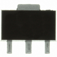
MMG3H21NT1 Freescale Semiconductor, MMG3H21NT1 Datasheet

MMG3H21NT1
Specifications of MMG3H21NT1
Available stocks
Related parts for MMG3H21NT1
MMG3H21NT1 Summary of contents
Page 1
... Heterojunction Bipolar Transistor Technology (InGaP HBT) Broadband High Linearity Amplifier The MMG3H21NT1 is a General Purpose Amplifier that is internally input matched and internally output matched designed for a broad range of Class A, small - signal, high linearity, general purpose applica- tions suitable for applications with frequencies from 0 to 6000 MHz such as Cellular, PCS, BWA, WLL, PHS, CATV, VHF, UHF, UMTS and general small - signal RF ...
Page 2
... Output Return Loss (S22) Power Output @ 1dB Compression Third Order Output Intercept Point Noise Figure (1) Supply Current (1) Supply Voltage 1. For reliable operation, the junction temperature should not exceed 150°C. MMG3H21NT1 Vdc, 900 MHz 25°C, 50 ohm system, in Freescale Application Circuit Symbol G p ...
Page 3
... Machine Model (per EIA/JESD 22 - A115) Charge Device Model (per JESD 22 - C101) Table 7. Moisture Sensitivity Level Test Methodology Per JESD 22 - A113, IPC/JEDEC J - STD - 020 RF Device Data Freescale Semiconductor Figure 1. Functional Diagram Class 1C (Minimum) A (Minimum) IV (Minimum) Rating Package Peak Temperature 1 260 Unit °C MMG3H21NT1 3 ...
Page 4
... OUTPUT POWER (dBm) out Figure 4. Small - Signal Gain versus Output Power 160 140 120 100 COLLECTOR VOLTAGE (V) CC Figure 6. Collector Current versus Collector Voltage MMG3H21NT1 4 50 OHM TYPICAL CHARACTERISTICS 0 − −40°C C −20 85°C 25°C −30 − Figure 3. Input/Output Return Loss versus Vdc CC I ...
Page 5
... Input Signal PAR = 8 0.01% Probability (CCDF) −40 −50 − Vdc − Figure 13. Single - Carrier W - CDMA Adjacent Channel Power Ratio versus Output Power = 5 Vdc TEMPERATURE (_C) versus Case Temperature 125 130 135 140 145 T , JUNCTION TEMPERATURE (° Vdc mA 2140 MHz OUTPUT POWER (dBm) out MMG3H21NT1 100 150 20 5 ...
Page 6
... FREQUENCY (MHz) Figure 15. S21, S11 and S22 versus Frequency Table 8. 50 Ohm Test Circuit Component Designations and Values Part C1, C2, C3 0.1 μF Chip Capacitors C4 1 μF Chip Capacitor L1 470 nH Chip Inductor R1 0 Ω Chip Resistor MMG3H21NT1 6 V SUPPLY DUT 0.403″ x 0.058″ Microstrip PCB Getek Grade ML200C, 0.031″ ...
Page 7
... Getek Grade ML200C, 0.031″, ε Figure 17. 50 Ohm Test Circuit Schematic C1 2800 3300 3800 Figure 19. 50 Ohm Test Circuit Component Layout Description C4 RF OUTPUT 4 MMG30XX Rev 2 Part Number Manufacturer C0603C104J5RAC Kemet C0603C105J5RAC Kemet C0603C105J5RAC Kemet HK160856NJ - T Taiyo Yuden ERJ3GEY0R00V Panasonic MMG3H21NT1 7 ...
Page 8
... Recommended Solder Stencil Figure 20. Recommended Mounting Configuration MMG3H21NT1 8 5.33 1.27 NOTES: 1. THERMAL AND RF GROUNDING CONSIDERATIONS SHOULD BE USED IN PCB LAYOUT DESIGN. 2. DEPENDING ON PCB DESIGN RULES, AS MANY VIAS AS POSSIBLE SHOULD BE PLACED ON THE LANDING PATTERN VIAS CANNOT BE PLACED ON THE LANDING PATTERN, THEN ...
Page 9
... MMG3H21NT1 9 ...
Page 10
... MMG3H21NT1 10 50 OHM TYPICAL CHARACTERISTICS ( Vdc mA 25°C, 50 Ohm System) (continued ∠ φ 6.440 74.9 0.0558 6.356 73.1 ...
Page 11
... RF Device Data Freescale Semiconductor PACKAGE DIMENSIONS MMG3H21NT1 11 ...
Page 12
... MMG3H21NT1 12 RF Device Data Freescale Semiconductor ...
Page 13
... RF Device Data Freescale Semiconductor MMG3H21NT1 13 ...
Page 14
... Application Notes • AN1955: Thermal Measurement Methodology of RF Power Amplifiers • AN3100: General Purpose Amplifier Biasing The following table summarizes revisions to this document. Revision Date 0 Apr. 2008 • Initial Release of Data Sheet MMG3H21NT1 14 PRODUCT DOCUMENTATION REVISION HISTORY Description RF Device Data Freescale Semiconductor ...
Page 15
... Denver, Colorado 80217 1 - 800 - 441 - 2447 or 303 - 675 - 2140 Fax: 303 - 675 - 2150 LDCForFreescaleSemiconductor@hibbertgroup.com RF Device Data Document Number: MMG3H21NT1 Rev. 0, 4/2008 Freescale Semiconductor Information in this document is provided solely to enable system and software implementers to use Freescale Semiconductor products. There are no express or implied copyright licenses granted hereunder to design or fabricate any integrated circuits or integrated circuits based on the information in this document ...


