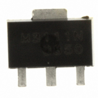
MMH3111NT1 Freescale Semiconductor, MMH3111NT1 Datasheet

MMH3111NT1
Specifications of MMH3111NT1
MMH3111NT1TR
Available stocks
Related parts for MMH3111NT1
MMH3111NT1 Summary of contents
Page 1
... Heterostructure Field Effect Transistor (GaAs HFET) Broadband High Linearity Amplifier The MMH3111NT1 is a General Purpose Amplifier that is internally input and output prematched designed for a broad range of Class A, small--signal, high linearity, general purpose applications suitable for applications with frequencies from 250 to 4000 MHz such as Cellular, PCS, WLL, PHS, CATV, VHF, UHF, UMTS and general small--signal RF ...
Page 2
... Output Return Loss (S22) Power Output @ 1dB Compression Third Order Output Intercept Point Noise Figure (1) Supply Current (1) Supply Voltage 1. For reliable operation, the junction temperature should not exceed 150°C. MMH3111NT1 Vdc, 900 MHz 25°C, 50 ohm system, in Freescale Application Circuit Symbol G p ...
Page 3
... Machine Model (per EIA/JESD 22--A115) Charge Device Model (per JESD 22--C101) Table 7. Moisture Sensitivity Level Test Methodology Per JESD 22--A113, IPC/JEDEC J--STD--020 RF Device Data Freescale Semiconductor Figure 1. Functional Diagram Class 1A (Minimum) A (Minimum) IV (Minimum) Rating Package Peak Temperature 1 260 Unit °C MMH3111NT1 3 ...
Page 4
... P , OUTPUT POWER (dBm) out Figure 4. Small- -Signal Gain versus Output Power 160 140 120 100 DRAIN VOLTAGE (V) DD Figure 6. Drain Current versus Drain Voltage MMH3111NT1 4 50 OHM TYPICAL CHARACTERISTICS 0 --10 --20 25°C -- Vdc DD -- Figure 3. Input/Output Loss versus Frequency Vdc 150 mA DD ...
Page 5
... Channel Power Ratio versus Output Power Vdc 900 MHz, 10 dBm per Tone DD Two--Tone Measurements, 1 MHz Tone Spacing TEMPERATURE (_C) versus Case Temperature 125 130 135 140 145 T , JUNCTION TEMPERATURE (° Vdc 150 150 mA 2140 MHz OUTPUT POWER (dBm) out MMH3111NT1 100 150 ...
Page 6
... Part C1 Chip Capacitors C3 0.1 μF Chip Capacitor C4 1 μF Chip Capacitor C5 0.7 pF Chip Capacitor C6 0.4 pF Chip Capacitor Chip Inductor Chip Inductor R1 0 Ω, 1/10 W Chip Resistor MMH3111NT1 6 V SUPPLY R1 L1 DUT 0.403″ x 0.058″ Microstrip Z7 0.086″ x 0.058″ Microstrip Z8 0.261″ ...
Page 7
... Figure 17. 50 Ohm Test Circuit Schematic Vdc 150 mA DD 2200 2300 Figure 19. 50 Ohm Test Circuit Component Layout Description 06035J470BBS C0603C104J5RAC C0603C105J5RAC 06035J0R7BBS 12105J0R4BBS HK160856NJ--T CRCW06030000FKEA OUTPUT 4 MMG30XX Rev 2 Part Number Manufacturer AVX Kemet Kemet AVX AVX Taiyo Yuden Vishay MMH3111NT1 C6 7 ...
Page 8
... Part C1 Chip Capacitors C3 0.1 μF Chip Capacitor C4 1 μF Chip Capacitor C5 0.8 pF Chip Capacitor C6 0.4 pF Chip Capacitor Chip Inductor R1 0 Ω, 1/10 W Chip Resistor MMH3111NT1 8 DUT 0.075″ x 0.058″ Microstrip Z6 0.403″ x 0.058″ Microstrip Z7 0.347″ x 0.058″ Microstrip PCB Getek Grade ML200C, 0.031″ ...
Page 9
... MMH3111NT1 9 ...
Page 10
... MMH3111NT1 10 50 OHM TYPICAL CHARACTERISTICS ( Vdc 150 mA 25°C, 50 Ohm System) (continued ∠ φ 3.502 89.764 0.120 3.480 87 ...
Page 11
... POSSIBLE SHOULD BE PLACED ON THE LANDING PATTERN VIAS CANNOT BE PLACED ON THE LANDING PATTERN, THEN AS MANY VIAS AS POSSIBLE SHOULD BE PLACED AS CLOSE TO THE LANDING PATTERN AS POSSIBLE FOR OPTIMAL THERMAL AND RF PERFORMANCE. 4. RECOMMENDED VIA PATTERN SHOWN HAS 0.381 x 0.762 MM PITCH. 7.62 0.305 diameter 2.49 2.54 MMH3111NT1 11 ...
Page 12
... MMH3111NT1 12 PACKAGE DIMENSIONS RF Device Data Freescale Semiconductor ...
Page 13
... RF Device Data Freescale Semiconductor MMH3111NT1 13 ...
Page 14
... MMH3111NT1 14 RF Device Data Freescale Semiconductor ...
Page 15
... Apr. 2010 • Changed Maximum Ratings table value for RF input power from dBm as a result of improvements made in the measurement method and the capability of the device • Added .s2p File availability to Product Software Device Data Freescale Semiconductor REVISION HISTORY Description MMH3111NT1 15 ...
Page 16
... Freescale Semiconductor Literature Distribution Center 1--800--441--2447 or +1--303--675--2140 Fax: +1--303--675--2150 LDCForFreescaleSemiconductor@hibbertgroup.com MMH3111NT1 Document Number: MMH3111NT1 Rev. 2, 4/2010 16 Information in this document is provided solely to enable system and software implementers to use Freescale Semiconductor products. There are no express or implied copyright licenses granted hereunder to design or fabricate any integrated circuits or integrated circuits based on the information in this document ...


