MW4IC2230NBR1 Freescale Semiconductor, MW4IC2230NBR1 Datasheet
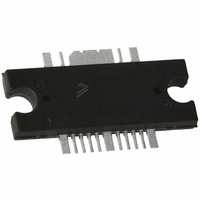
IC PWR AMP RF 28V 30W TO272-16

MW4IC2230NBR1

Manufacturer Part Number
MW4IC2230NBR1
Description
IC PWR AMP RF 28V 30W TO272-16
Manufacturer
Freescale Semiconductor
Type
Power Amplifierr
Datasheet

Specifications of MW4IC2230NBR1

Current - Supply
60mA
Frequency
1.6GHz ~ 2.4GHz
Gain
31dB
Package / Case
TO-272-16
Rf Type
Cellular, CDMA, EDGE, GSM, TDMA, W-CDMA
Voltage - Supply
26V
Number Of Channels
1
Frequency (max)
2.17GHz
Power Supply Requirement
Single
Single Supply Voltage (min)
26V
Single Supply Voltage (max)
28V
Dual Supply Voltage (min)
Not RequiredV
Dual Supply Voltage (typ)
Not RequiredV
Dual Supply Voltage (max)
Not RequiredV
Pin Count
16
Mounting
Surface Mount
Lead Free Status / RoHS Status
Lead free / RoHS Compliant
Noise Figure
-
P1db
-
Test Frequency
-
Lead Free Status / Rohs Status
Compliant
Other names
MW4IC2230NBR1TR

Available stocks

Company
Part Number
Manufacturer
Quantity
Price
Part Number:
MW4IC2230NBR1
Manufacturer:
FREESCALE
Quantity:
20 000
Company:
Part Number:
MW4IC2230NBR1
Quantity:
650
© Freescale Semiconductor, Inc., 2006. All rights reserved.
RF Device Data
Freescale Semiconductor
Technical Data
RF LDMOS Wideband Integrated
Power Amplifiers
base station applications. It uses Freescale’s newest High Voltage (26 to 28
Volts) LDMOS IC technology and integrates a multi - stage structure. Its
wideband on- chip design makes it usable from 1600 to 2400 MHz. The linearity
performances cover all modulations for cellular applications: GSM, GSM
EDGE, TDMA, CDMA and W - CDMA.
Final Application
• Typical Single - Carrier W - CDMA Performance:
Driver Application
• Typical Single - Carrier W - CDMA Performance:
• Capable of Handling 3:1 VSWR, @ 28 Vdc, 2170 MHz, 5 Watts CW
• Stable into a 3:1 VSWR. All Spurs Below - 60 dBc @ 10 mW to 5 W CW
• Characterized with Series Equivalent Large - Signal Impedance Parameters
• On - Chip Matching (50 Ohm Input, DC Blocked, >5 Ohm Output)
• Integrated Quiescent Current Temperature Compensation
• On - Chip Current Mirror g
• Integrated ESD Protection
• 200°C Capable Plastic Package
• In Tape and Reel. R1 Suffix = 500 Units per 44 mm, 13 inch Reel
1. Refer to AN1987, Quiescent Current Control for the RF Integrated Circuit Device Family. Go to http://www.freescale.com/rf.
The MW4IC2230M wideband integrated circuit is designed for W - CDMA
60 mA, I
Bandwidth = 3.84 MHz, PAR = 8.5 dB @ 0.01% Probability on CCDF.
60 mA, I
Bandwidth = 3.84 MHz, PAR = 8.5 dB @ 0.01% Probability on CCDF.
Output Power
P
with Enable/Disable Function
Select Documentation/Application Notes - AN1987.
out
Power Gain — 31 dB
Drain Efficiency — 15%
ACPR @ 5 MHz = - 45 dBc in 3.84 MHz Bandwidth
Power Gain — 31.5 dB
ACPR @ 5 MHz = - 53.5 dBc in 3.84 MHz Bandwidth
.
V
V
V
V
V
V
V
RF
RD1
RG1
GS1
GS2
GS3
DS2
DS1
in
DQ2
DQ2
= 350 mA, P
= 350 mA, P
Figure 1. Functional Block Diagram
Replaced by MW4IC2230NBR1(GNBR1). There are no form, fit or function changes with this
part replacement. N suffix added to part number to indicate transition to lead - free terminations.
out
out
m
Reference FET for Self Biasing Application
Temperature Compensation
= 5 Watts Avg., f = 2140 MHz, Channel
= 0.4 Watts Avg., f = 2140 MHz, Channel
Quiescent Current
3 Stages I
V
V
C
DD
DD
= 28 Volts, I
= 28 Volts, I
DQ1
DQ1
V
=
=
DS3
(1)
/RF
out
INTEGRATED POWER AMPLIFIERS
MW4IC2230MBR1 MW4IC2230GMBR1
MW4IC2230GMBR1
Note: Exposed backside flag is source
Document Number: MW4IC2230
MW4IC2230MBR1
2110 - 2170 MHz, 30 W, 28 V
V
V
V
GND
V
V
V
V
GND
Figure 2. Pin Connections
RF
RF LDMOS WIDEBAND
TO - 272 WB - 16 GULL
GS1
GS2
GS3
DS2
RD1
RG1
DS1
MW4IC2230GMBR1
in
terminal for transistors.
CASE 1329A - 03
SINGLE W - CDMA
PLASTIC
MW4IC2230MBR1
10
11
1
2
3
4
5
6
7
8
9
TO - 272 WB - 16
CASE 1329 - 09
(Top View)
PLASTIC
16
15
14
13
12
Rev. 5, 5/2006
GND
V
RF
GND
DS3/
out
1

Related parts for MW4IC2230NBR1

MW4IC2230NBR1 Summary of contents

Page 1

... Freescale Semiconductor Technical Data Replaced by MW4IC2230NBR1(GNBR1). There are no form, fit or function changes with this part replacement. N suffix added to part number to indicate transition to lead - free terminations. RF LDMOS Wideband Integrated Power Amplifiers The MW4IC2230M wideband integrated circuit is designed for W - CDMA base station applications. It uses Freescale’s newest High Voltage ( Volts) LDMOS IC technology and integrates a multi - stage structure ...

Page 2

... I = 350 mA, DD DQ1 DQ2 — 43 — — ±5 — — 0.13 — — ±1 — — 1.6 — — ±15 — (continued) RF Device Data Freescale Semiconductor Unit Vdc Vdc °C °C dBm Unit Unit °C Unit dB dB dBc ° ns ° ...

Page 3

... MHz Channel Bandwidth @ ±10 MHz Offset. PAR = 8 0.01% Probability on CCDF. Power Gain Intermodulation Distortion Adjacent Channel Power Ratio Input Return Loss RF Device Data Freescale Semiconductor (continued) = 25°C unless otherwise noted) C Symbol = 245 mA 2112.5 MHz 2122.5 MHz and f1 = 2157.5 MHz 2167.5 MHz, ...

Page 4

... Quiescent Current 9 Temperature Compensation 1.120″ x 0.090″ Microstrip Z7 0.340″ x 0.090″ Microstrip PCB Taconic TLX8 - 0300, 0.030″, ε Description OUTPUT C10 C11 C12 2.55 r Part Number Manufacturer TAJD106K035 AVX 100B8R2CW ATC 100B1R8BW ATC 100B0R3BW ATC RF Device Data Freescale Semiconductor RF ...

Page 5

... Freescale has begun the transition of marking Printed Circuit Boards (PCBs) with the Freescale Semiconductor signature/logo. PCBs may have either Motorola or Freescale markings during the transition period. These changes will have no impact on form, fit or function of the current product. Figure 4. MW4IC2230MBR1(GMBR1) Test Circuit Component Layout ...

Page 6

... FREQUENCY (MHz −10 −20 IRL −30 −40 −50 ACPR − 85_C C = 350 mA 265 mA DQ2 DQ3 25_C −30_C OUTPUT POWER (WATTS) AVG. out versus Output Power 0 − −20 IRL −30 −40 IM3 −50 ACPR −60 RF Device Data Freescale Semiconductor 10 ...

Page 7

... P , INPUT POWER (dBm) in Figure 9. Output Power versus Input Power 1.E+09 1.E+08 1.E+07 1.E+06 1.E+05 1.E+04 Figure 11. MTTF Factor versus Temperature Junction RF Device Data Freescale Semiconductor TYPICAL CHARACTERISTICS 2.00 Ideal 1.95 1.90 Actual 1.85 1.80 1.75 1.70 1.65 = 265 mA, 1.60 DQ3 1.55 1 ...

Page 8

... Device input impedance as measured from gate to ground. = Test circuit impedance as measured from drain to ground. Output Device Matching Under Network Test load = 26 dBm out Ω RF Device Data Freescale Semiconductor ...

Page 9

... RF Device Data Freescale Semiconductor NOTES MW4IC2230MBR1 MW4IC2230GMBR1 9 ...

Page 10

... MW4IC2230MBR1 MW4IC2230GMBR1 10 PACKAGE DIMENSIONS RF Device Data Freescale Semiconductor ...

Page 11

... RF Device Data Freescale Semiconductor MW4IC2230MBR1 MW4IC2230GMBR1 11 ...

Page 12

... MW4IC2230MBR1 MW4IC2230GMBR1 12 RF Device Data Freescale Semiconductor ...

Page 13

... RF Device Data Freescale Semiconductor MW4IC2230MBR1 MW4IC2230GMBR1 13 ...

Page 14

... MW4IC2230MBR1 MW4IC2230GMBR1 14 RF Device Data Freescale Semiconductor ...

Page 15

... RF Device Data Freescale Semiconductor MW4IC2230MBR1 MW4IC2230GMBR1 15 ...

Page 16

... Freescale Semiconductor product could create a situation where personal injury or death may occur. Should Buyer ...

Related keywords