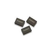
MGA-645T6-TR1G Avago Technologies US Inc., MGA-645T6-TR1G Datasheet

MGA-645T6-TR1G
Specifications of MGA-645T6-TR1G
Available stocks
Related parts for MGA-645T6-TR1G
MGA-645T6-TR1G Summary of contents
Page 1
... Ultra Thin Package. The compact footprint and low profile coupled with low noise, high linearity make the MGA-645T6 an ideal choice as a low noise amplifier for mobile receiver in the WiMax, WLAN(802.11b/g), WiBro and DMB applications. ...
Page 2
Absolute Maximum Rating TA=25°C Symbol Parameter Vdd Device Voltage V Control Voltage bypass Input Power in,max P Total Power Dissipation diss T Junction Temperature j T Storage Temperature STG Product Consistency Distribution Charts Figure 1. Gain ...
Page 3
Demo Board Layout VBYPASS J1 VDD GROUND Figure 4. Demo Board Layout Diagram * 1.2 1.4 1.6 1.8 2 2.2 Vsd,V Figure Vbypass (Vdd=3V ...
Page 4
... Demo Board Schematic for 2.3–2.4 GHz tuning MGA-645T6 1 Vbypass bias/control 2 RFin 3 L1 Figure 6. Demo Board Schematic Diagram MGA-645T6 Typical Performance (2.3 – 2.4 GHz match +25 °C, Vdd = 3V, Ids = 7mA (Vbypass = 1.8V), RF measurement at 2.4 GHz, Input Signal=CW unless stated otherwise -10 -20 -30 -40 ...
Page 5
LNA Mode Plots (2.3 – 2.4 GHz match) ; Vdd = 3V 2 1.8 1.6 1.4 1.2 1 0.8 0.6 0.4 0 2.2 2.4 2.6 Freq,GHz Figure 8. LNA Mode Noise Figure vs Frequency 16.5 ...
Page 6
Bypass Mode Plots (2.3 – 2.4 GHz match) (Vdd = 3V ; Vbypass = 0V -10 -15 -20 Output Return Loss -25 -30 -35 -40 -45 1.0 1.5 2.0 2.5 Figure 14. Bypass Mode S21, S11, S22, S12 ...
Page 7
... Demo Board Schematic for 2.5 – 2.7 GHz tuning MGA-645T6 1 Vbypass bias/control 2 RFin 3 L1 Figure 18. Demo Board Schematic Diagram MGA-645T6 Typical Performance (2.5 GHz – 2.7 GHz match +25 °C, Vdd = 3V, Ids = 7mA (Vbypass = 1.8V), RF measurement at 2.6 GHz, Input Signal=CW unless stated otherwise Output Return Loss 0 -10 Input Return Loss -20 ...
Page 8
LNA Mode Plots (2.5 – 2.7 GHz match) ; Vdd = 3V 2 1.8 1.6 1.4 1.2 1 0.8 0.6 0.4 0 2.2 2.4 2.6 Freq,GHz Figure 20. LNA Mode Noise Figure vs Frequency 16.5 ...
Page 9
Bypass Mode Plots (2.5 – 2.7 GHz match) (Vdd=3V; Vbypass = 0V) 0 Input Return Loss -5 -10 -15 Output Return Loss -20 -25 -30 1.0 1.5 2.0 2.5 Figure 26. Bypass Mode S21, S11, S22, S12 vs Frequency -3 ...
Page 10
... Test Circuit For S and Noise parameter measurement Reference plane MGA-645T6 1 Vbypass bias/control 2 RFin 3 Figure 30. S parameter and Noise parameter test circuit in an automated measurement system MGA-645T6 LNA Mode typical scattering parameters at 25C, Vdd = 7mA Freq. S11 (GHz) Mag Ang 0.5 0.967 -24.335 1 ...
Page 11
... MGA-645T6 LNA Mode typical noise parameters at 25 Freq.(GHz) Fmin (dB) 2 0.55 2.1 0.57 2.2 0.59 2.3 0.62 2.4 0.72 2.5 0.75 2.6 0.78 2.7 2.8 0.83 2.9 0.85 3 0.88 3.1 0.91 3.2 0.95 3.3 0.98 3.4 1.02 3.5 1.06 3.6 1 ...
Page 12
... MGA-645T6 Bypass Mode typical scattering parameters at 25 Freq. S11 (GHz) Mag Ang 0.5 0.95 -31.2 1 0.925 -48.1 1.5 0.9 -65 2 0.875 -81.9 2.1 0.87 -85.28 2.2 0.855 -88.66 2.3 0.849 -91.44 2.4 0.842 -94.52 2.5 0.838 -97.2 2.6 0.831 -100.18 2.7 ...
Page 13
Package Dimensions PIN #1 DOT BY MARKING ± 2.00 0.05 ± 1.30 0.05 PCB Land Pattern 1.700 1.100 0.435 0.300 0.350 0.350 0.230 0.310 0.332 Land Pattern With Via Stencil Outline Drawing and Combined Land Pattern & Stencil Layout 1.960 ...
Page 14
... COVER TAPE Tape Dimensions 4.0 ± 0.10 4.0 ± 0.10 8.00 +0.30/-0.10 0. ± Part Number Ordering Information Part # Qty MGA-645T6-BLKG 100 MGA-645T6-TR1G 3000 MGA-645T6-TR2G 10000 14 CARRIER TAPE 2.00 ± 0.05 0.20 ± 0.15 45° MAX. 0.73 ± 0.05 Container Antistatic Bag 7” ...
Page 15
Reel Dimensions - 7 Inch 6.25mm EMBOSSED LETTERS LETTERING THICKNESS: 1.6mm SEE DETAIL "X" SLOT HOLE "b" SLOT HOLE(2x) 180° APART FRONT VIEW RECYCLE LOGO R10.65 R5.2 Slot hole 'b' EMBOSSED RIBS RAISED: 0.25mm, WIDTH: 1.25mm BACK VIEW ...
Page 16
DATE CODE EMBOSSED LETTERING 7.5mm HEIGHT EMBOSSED LINE (2x) 89.0mm LENGTH LINES 147.0mm AWAY FROM CENTER POINT ESD LOGO 6 PS RECYCLE LOGO SEE DETAIL "X" For product ...


