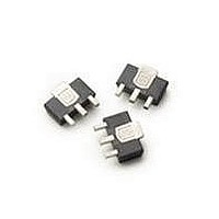
MGA-30989-BLKG Avago Technologies US Inc., MGA-30989-BLKG Datasheet

MGA-30989-BLKG
Specifications of MGA-30989-BLKG
Related parts for MGA-30989-BLKG
MGA-30989-BLKG Summary of contents
Page 1
... The device required simple dc biasing components to achieve wide bandwidth performance. The temperature compensated internal bias circuit provides stable current over temperature and process threshold voltage variation. The MGA-30989 is housed inside a low cost RoHS compliant SOT89 industry standard SMT package (4.5 x 4.1 x 1.5 mm). Component Image ...
Page 2
Absolute Maximum Rating T =25°C A Symbol Parameter V Device Voltage, RF output to ground dd,max Input Power in,max [3] P Total Power Dissipation diss T Junction Temperature j,MAX T Storage Temperature STG Product Consistency Distribution ...
Page 3
Electrical Specifications T = 25°C, Vdd = 5V A Symbol Parameter and Test Condition Ids Quiescent current Gain Gain [2] OIP3 Output Third Order Intercept Point NF Noise Figure S11 Input Return Loss, 50: source S22 Output Return Loss, ...
Page 4
Typical Performance (2GHz - 4GHz 25°C, Vdd = 5V, Input Signal = CW. Application Test Circuit is shown in Figure 22 and Table Temperature (°C) Figure 6. Ids over Temperature ...
Page 5
Typical Performance (2GHz - 4GHz 25°C, Vdd = 5V, Input Signal = CW. Application Test Circuit is shown in Figure 22 and Table 1. A -16 -18 -20 -22 -24 -26 -28 -30 Frequency (GHz) Figure 12. S12 ...
Page 6
Typical Performance (3GHz - 6GHz 25°C, Vdd = 5V, Input Signal = CW. Application Test Circuit is shown in Figure 22 and Table -10 -15 -20 -25 -30 Frequency (GHz) Figure 18. S11 over ...
Page 7
Application Schematic Components Table and Demo Board C14 C7 RFin RFin 1 Figure 22. Application Schematic C14 Figure 23. Demo board Layout 7 Vdd C1 Top View L1 Vdd C8 GND 2 RFout 3 C13 – Recommended PCB material is ...
Page 8
Demo board Part List Table 1. 2GHz - 4GHz Application Schematic Components Circuit Symbol Size L1 0603 C1 0402 C2 0402 C3 0805 C7 0402 C8 0402 C13 0402 C14 0402 Table 2. 3GHz - 6GHz Application Schematic Components Circuit ...
Page 9
Typical S-Parameter (Vdd = 5V 25°C, 50 ohm) A S11 S11 Freq (GHz) (dB) (ang) 0.1 -0.83 171.33 0.5 -0.85 133.94 1 -1.73 69.70 1.5 -18.64 13.90 2 -16.77 21.81 2.2 -17.69 26.98 2.4 -17.47 27.84 2.6 -17.54 ...
Page 10
... Dimensioning and tolerancing per ANSI.Y14.5M-1982 2. Controlling dimension: Millimeter convertions to inches are not necessarily exact 3. Dimension B1, 2 places 25°C, 50 ohm) Part Number Ordering Information * Part Number Ang R /Z opt n 0 MGA-30989-BLKG 49 0.52 MGA-30989-TR1G 90 0.29 122 0.19 174 0.18 -145 0.17 -103 0.21 -62 0 ...
Page 11
Device Orientation REEL USER FEED COVER TAPE DIRECTION Tape Dimensions 8.00±0.10 Ø1.50±0.10 (0.315±0.004) (0.059±0.004) 12.0±0.30–0.10 (0.472+0.012–0.004) 8° 4.80±0.10 (0.180±0.004) Dimensions in mm (inches) 11 9GX CARRIER TAPE 4.00±0.10 (0.157±0.004) (0.069±0.004) + Ø1.50±0.25 (0.059±0.010) 0.292±0.02 (0.0115±0.0008) 0.180±0.10 (0.0709±0.004) 4.40±0.10 (0.1732±0.004) 9GX ...
Page 12
Reel Dimensions – 13” Reel 12mm width DATE CODE EMBOSSED LETTERING 7.5mm HEIGHT EMBOSSED LINE (2x) 89.0mm LENGTH LINES 147.0mm AWAY FROM CENTER POINT ESD LOGO 6 PS ...


