MGA-425P8-TR2 Avago Technologies US Inc., MGA-425P8-TR2 Datasheet
MGA-425P8-TR2
Specifications of MGA-425P8-TR2
Available stocks


Related parts for MGA-425P8-TR2


MGA-425P8-TR2 Summary of contents
Page 1
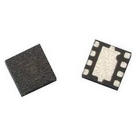
... PA has a high power efficiency (PAE) achieved through the use of Avago Technologies’s proprietary GaAs Enhancement- mode pHEMT process. MGA-425P8 is housed in a miniature 2.0 x 2.0 x 0.75 mm 8-lead leadless-plastic-chip-carrier (LPCC) package. The compact foot- print, low profile couple with the excellent thermal efficiency of the LPCC package makes the MGA-425P8 an ideal choice as power amplifier that saves board space ...
Page 2
... MGA-425P8 Absolute Maximum Ratings [1] Symbol Parameter V Drain – Supply Voltage [ Drain Current [ Total Power Dissipation [3] diss P max. RF Input Power in T Channel Temperature CH T Storage Temperature STG θ Thermal Resistance [4] ch_b Product Consistency Distribution Charts at 5.25 GHz, 3.3V RBias = 680Ω 150 ...
Page 3
... MGA-425P8 Electrical Specifications T = 25°C, DC bias for RF parameter is Vds = 3.3V and R A Symbol Parameter and Test Condition I Device Current ds G Gain [1] NF Noise Figure [1] OIP3 Output 3 Order Intercpt Point rd 32.9 – P1dB Output 1dB Compressed [1] PAE Power Added Efficiency [1] EVM Error Vector Magnitude at Pout=13 ...
Page 4
... MGA-425P8 Typical Performance Curves, Vds = 3.3V, Ids = 58 mA (at 25°C unless specified otherwise -40°C 28 +25°C +85° 2.5 3 3.5 4 4.5 5 5.5 6 FREQUENCY (GHz) Figure 7. OIP3 vs. Temperature and Frequency. 1.8 1.6 1.4 1.2 1 0.8 Vd=4V Ids=60 mA Vd=3.3 Ids=65 mA 0.6 Vd=3.3V Ids=80 mA 0.4 ...
Page 5
... MGA-425P8 Typical Performance Curves, Vds = 3.3V (at 25°C unless specified otherwise 100 IDS (mA) Figure 12. OIP3 vs. Ids at 5.25 GHz. 1.8 1.6 1.4 1.2 1 Vd=4V 0.8 Vd=3.3V 0.6 0 100 IDS (mA) Figure 15. FMIN vs. Ids at 5.25 GHz 100 IDS (mA) Figure 13. P1dB vs. Ids at 5.25 GHz 100 ...
Page 6
... MGA-425P8 Typical Scattering Parameters (at 25°C, V Freq GHz Mag. Ang. dB 0.1 0.806 -15.3 24.42 0.5 0.789 -59 22.96 0.9 0.799 -92.7 21.38 1 0.8 -99.5 20.95 1.5 0.814 -126.2 18.87 1.9 0.819 -141.1 17.34 2 0.823 -144.8 16.94 2.4 0.824 -155.7 15.56 3 0.828 -168.1 13 ...
Page 7
... MGA-425P8 Typical Scattering Parameters (at 25°C, V Freq GHz Mag. Ang. dB 0.1 0.8 -16.1 26.67 0.5 0.791 -63.6 25.06 0.9 0.806 -98.2 23.26 1 0.807 -105 22.79 1.5 0.822 -131 20.55 1.9 0.828 -145.2 18.97 2 0.832 -148.7 18.56 2.4 0.835 -159 17.15 3 0.841 -170 ...
Page 8
... MGA-425P8 Typical Scattering Parameters (at 25°C, V Freq GHz Mag. Ang. dB 0.1 0.796 -16.4 27.39 0.5 0.792 -65.5 25.72 0.9 0.807 -100.5 23.83 1 0.809 -107.2 23.34 1.5 0.825 -132.9 21.04 1.9 0.83 -146.9 19.42 2 0.836 -150.3 19.01 2.4 0.838 -160.3 17.58 3 0.844 -171 ...
Page 9
... MGA-425P8 Typical Scattering Parameters (at 25°C, V Freq GHz Mag. Ang. dB 0.1 0.795 -16.4 27.50 0.5 0.792 -65.6 25.84 0.9 0.808 -100.7 23.94 1 0.81 -107.5 23.44 1.5 0.825 -133.1 21.13 1.9 0.83 -147 19.51 2 0.836 -150.4 19.10 2.4 0.838 -160.4 17.68 3 0.844 -171 ...
Page 10
... MGA-425P8 Typical Scattering Parameters (at 25°C, V Freq GHz Mag. Ang. dB 0.1 0.79 -16.3 27.73 0.5 0.79 -65.7 26.07 0.9 0.807 -100.8 24.18 1 0.809 -107.6 23.68 1.5 0.825 -133.2 21.36 1.9 0.83 -147.1 19.75 2 0.835 -150.5 19.34 2.4 0.839 -160.4 17.91 3 0.845 -171 ...
Page 11
... MGA-425P8 Typical Scattering Parameters (at 25°C, V Freq GHz Mag. Ang. dB 0.1 0.797 -16.4 27.38 0.5 0.793 -65.7 25.70 0.9 0.809 -100.8 23.80 1 0.81 -107.5 23.31 1.5 0.826 -133.2 21.00 1.9 0.83 -147 19.39 2 0.836 -150.5 18.98 2.4 0.839 -160.4 17.56 3 0.844 -171 ...
Page 12
... MGA-425P8 Typical Scattering Parameters (at 25°C, V Freq GHz Mag. Ang. dB 0.1 0.796 -16.5 27.47 0.5 0.793 -66 25.79 0.9 0.809 -101.1 23.88 1 0.811 -107.8 23.38 1.5 0.826 -133.4 21.06 1.9 0.832 -147.3 19.45 2 0.836 -150.6 19.04 2.4 0.839 -160.6 17.62 3 0.846 -172 15 ...
Page 13
... Device Models Refer to Avago’s Web Site www.Avagotech.com/view/rf Ordering Information Part Number No. of Devices MGA-425P8-TR1 3000 MGA-425P8-TR2 10000 MGA-425P8-BLK 100 LPCC (JEDEC DFP-N) Package Dimensions D1 pin1 Bottom View A2 A1 Side View DIMENSIONS (mm) SYMBOL MIN. NOM. MAX. A 0.70 0.75 0. 0.02 0.05 A2 0.203 REF b 0 ...
Page 14
PCB Land Pattern and Stencil Design 2.80 (110.24) 0.70 (27.56) 0.25 (9.84) 0.25 (9.84) PIN 1 0.20 (7.87) Solder + mask 0.60 (23.62) RF transmission 0.80 (31.50) line 0.15 (5.91) 0.55 (21.65) PCB Land Pattern (top view) Notes: Typical stencil ...
Page 15
Tape Dimensions Max ° DESCRIPTION CAVITY LENGTH WIDTH DEPTH PITCH BOTTOM HOLE DIAMETER PERFORATION DIAMETER PITCH POSITION CARRIER TAPE WIDTH THICKNESS COVER TAPE WIDTH TAPE THICKNESS DISTANCE CAVITY TO PERFORATION (WIDTH DIRECTION) ...