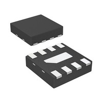
AMMP-6220-TR1 Avago Technologies US Inc., AMMP-6220-TR1 Datasheet

AMMP-6220-TR1
Specifications of AMMP-6220-TR1
Available stocks
Related parts for AMMP-6220-TR1
AMMP-6220-TR1 Summary of contents
Page 1
... Intended applications include microwave radios, 802.16, automotive radar, VSAT, and satellite receivers. Since one part can cover several bands, the AMMP-6220 can reduce part inventory and increase volume purchase options. The LNA has integrated 50 W I/O match, DC block- ...
Page 2
... AMMP-6220 Absolute Maximum Ratings Symbol Parameters/Conditions V Positive Drain Voltage d I Drain Current Input Power in T Operating Channel Temp Storage Case Temp. stg T Maximum Assembly Temp. max (60 sec max.) Note: 1. Operation in excess of any one of these conditions may result in permanent damage to this device. ...
Page 3
... AMMP-6220 Typical Performances (T = 25° Note: These measurements are test environment. Aspects of the amplifier performance may be improved over a narrower bandwidth by application of additional conjugate, linearity or low noise (Gopt) matching FREQUENCY (GHz) Figure 1. Gain -10 -15 -20 -25 - FREQUENCY (GHz) Figure 4. Output return loss +25°C 10 -40° ...
Page 4
... AMMP-6220 Typical Performances (T = 25° Note: These measurements are test environment. Aspects of the amplifier performance may be improved over a narrower bandwidth by application of additional conjugate, linearity or low noise (Gopt) matching. 0 +25°C -5 -40°C +85°C -10 -15 -20 -25 - FREQUENCY (GHz) Figure 10. Output return loss over temperature. ...
Page 5
... AMMP-6220 Typical Scattering Parameters S11 Freq GHz DB Mag Phase 2.0 -1.46 0.845 65.6 2.5 -1.03 0.888 -4.4 3.0 -0.40 0.955 -83.9 3.5 -4.65 0.585 -150.2 4.0 -1.67 0.825 153.6 4.5 -1.39 0.851 72.8 5.0 -2.80 0.724 18.7 5.5 -1.59 0.832 -65.0 6 ...
Page 6
Biasing and Operation The AMMC-6220 is normally biased with a single positive drain supply connected to both V D capacitors as shown in Figure 19. The recommended supply voltage important to have 0.1 µF bypass ...
Page 7
... Outline Drawing AMMP XXXX A 8 YWWDNN FRONT VIEW SYMBOL MIN. A 0.198 (5.03) B 0.0685 (1.74) DIMENSIONS ARE IN INCHES (MM) 0.114 (2.90) 0.011 (0.28) 0.018 (0.46 0.126 0.059 (3.2) (1.5) 0.100 (2.54) 0.029 (0.75) 5 0.016 (0.40) 0.100 (2.54) 0.93 (2.36) BACK VIEW DIMENSIONAL TOLERANCE FOR BACK VIEW: 0.002" (0.05 mm) ...
Page 8
... Recommended SMT Attachment The AMMP Packaged Devices are compatible with high volume surface mount PCB assembly processes. The PCB material and mounting pattern, as defined in the data sheet, optimizes RF performance and is strongly rec- ommended. An electronic drawing of the land pattern is available upon request from Avago Sales & Application Engineering ...
Page 9
... Verify that the profile will not expose device beyond these limits. AMMP-6220 Part Number Ordering Information Part Number Devices Per Container AMMP-6220-BLK 10 AMMP-6220-TR1 100 AMMP-6220-TR2 500 9 Solder Reflow Profile The most commonly used solder reflow method is ac- complished in a belt furnace using convection heat transfer ...
Page 10
... Avago, Avago Technologies, and the A logo are trademarks of Avago Technologies Limited in the United States and other countries. Data subject to change. Copyright © 2005-2008 Avago Technologies Limited. All rights reserved. Obsoletes 5989-4517EN AV02-0515EN - May 8, 2008 4 mm AMMP AMMP XXXX XXXX ∅1.55 ± 0.05 R 0.50 TYP. ...


