MW4IC915NBR1 Freescale Semiconductor, MW4IC915NBR1 Datasheet
MW4IC915NBR1
Specifications of MW4IC915NBR1
Available stocks


Related parts for MW4IC915NBR1

MW4IC915NBR1 Summary of contents
Page 1
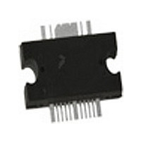
... MW4IC915NBR1 CASE 1329A - 272 GULL PLASTIC MW4IC915GNBR1 GND 1 GND RD2 RG2 V 4 DS1 V 5 RD1 RF out DS2 V 7 RG1 V 8 GS1 V 9 GS2 GND GND 12 11 (Top View) Note: Exposed backside flag is source terminal for transistors. Figure 2. Pin Connections MW4IC915NBR1 MW4IC915GNBR1 1 ...
Page 2
... MHz 869.1 MHz and f1 = 960 MHz and f2 = 960.1 MHz, Two - Tone Power Gain Power Added Efficiency Intermodulation Distortion Input Return Loss 1. Refer to AN1955/D, Thermal Measurement Methodology of RF Power Amplifiers http://www.freescale.com/rf. Select Documentation/Application Notes - AN1955. MW4IC915NBR1 MW4IC915GNBR1 2 Stage 1, 26 Vdc Stage 2, 26 Vdc 240 mA ...
Page 3
... I = 240 mA, DQ1 DQ2 — 20 — — 30 — — 44 — — — — 1.5 — — — — — MW4IC915NBR1 MW4IC915GNBR1 Unit % dB ° ns ° Watts rms dBc dBc 3 ...
Page 4
... Microstrip Z4 0.171″ x 0.283″ Microstrip Z5 0.429″ x 0.283″ Microstrip Figure 3. MW4IC915NBR1(GNBR1) Test Fixture Schematic Table 6. MW4IC915NBR1(GNBR1) Test Fixture Component Designations and Values Part C1, C6, C9, C14 22 mF Tantalum Chip Capacitors C2, C5, C8, C11 1000 pF Chip Capacitors C3, C4, C7, C10, C16 ...
Page 5
... Freescale has begun the transition of marking Printed Circuit Boards (PCBs) with the Freescale Semiconductor signature/logo. PCBs may have either Motorola or Freescale markings during the transition period. These changes will have no impact on form, fit or function of the current product. Figure 4. MW4IC915NBR1(GNBR1) Test Fixture Component Layout RF Device Data Freescale Semiconductor ...
Page 6
... Microstrip Z3 0.468″ x 0.157″ Microstrip Z4 0.220″ x 0.157″ Microstrip Figure 5. MW4IC915NBR1(GNBR1) Reference Board Schematic Table 7. MW4IC915NBR1(GNBR1) Reference Board Component Designations and Values Part C1, C15 10 pF Chip Capacitors (0805), ACCU - P C2 5.6 pF Chip Capacitor (0805), ACCU - P ...
Page 7
... Freescale has begun the transition of marking Printed Circuit Boards (PCBs) with the Freescale Semiconductor signature/logo. PCBs may have either Motorola or Freescale markings during the transition period. These changes will have no impact on form, fit or function of the current product. Figure 6. MW4IC915NBR1(GNBR1) Reference Board Component Layout RF Device Data Freescale Semiconductor ...
Page 8
... DQ1 DQ2 910 MHz 25_C 31 PAE 30 85_C 0 OUTPUT POWER (WATTS) out Figure 10. Power Gain and Power Added Efficiency versus Output Power MW4IC915NBR1 MW4IC915GNBR1 8 PAE IRL Vdc (PEP) out mA 240 mA DQ1 DQ2 Two−Tone Measurement 100 kHz Tone Spacing 880 900 920 ...
Page 9
... Vdc out mA 240 mA DQ1 DQ2 880 890 900 910 920 930 940 950 f, FREQUENCY (MHz) Frequency 25_C T = 85_C C −30_C Vdc mA 240 mA DQ1 DQ2 EDGE Modulation f = 910 MHz OUTPUT POWER (WATTS) out versus Output Power 85_C 25_C 100 MW4IC915NBR1 MW4IC915GNBR1 960 100 9 ...
Page 10
... Figure 17. Series Equivalent Input and Load Impedance MW4IC915NBR1 MW4IC915GNBR1 Ω load f = 900 MHz f = 980 MHz mA 240 mA P1dB DD DQ1 DQ2 out f Z load MHz Ω 900 3.23 - j4.30 910 3.24 - j4.36 920 3.25 - j4.42 930 3.25 - j4.47 940 3.23 - j4.52 950 3.21 - j4.56 960 3 ...
Page 11
... RF Device Data Freescale Semiconductor NOTES MW4IC915NBR1 MW4IC915GNBR1 11 ...
Page 12
... MW4IC915NBR1 MW4IC915GNBR1 12 NOTES RF Device Data Freescale Semiconductor ...
Page 13
... RF Device Data Freescale Semiconductor NOTES MW4IC915NBR1 MW4IC915GNBR1 13 ...
Page 14
... MW4IC915NBR1 MW4IC915GNBR1 14 PACKAGE DIMENSIONS RF Device Data Freescale Semiconductor ...
Page 15
... RF Device Data Freescale Semiconductor MW4IC915NBR1 MW4IC915GNBR1 15 ...
Page 16
... MW4IC915NBR1 MW4IC915GNBR1 16 RF Device Data Freescale Semiconductor ...
Page 17
... RF Device Data Freescale Semiconductor MW4IC915NBR1 MW4IC915GNBR1 17 ...
Page 18
... MW4IC915NBR1 MW4IC915GNBR1 18 RF Device Data Freescale Semiconductor ...
Page 19
... RF Device Data Freescale Semiconductor MW4IC915NBR1 MW4IC915GNBR1 19 ...
Page 20
... RoHS- compliant and/ free versions of Freescale products have the functionality and electrical characteristics of their non - RoHS- compliant and/or non - Pb- free counterparts. For further information, see http://www.freescale.com or contact your Freescale sales representative. For information on Freescale’s Environmental Products program http://www.freescale.com/epp. MW4IC915NBR1 MW4IC915GNBR1 MW4IC915N Rev. 7, 5/2006 20 Information in this document is provided solely to enable system and software implementers to use Freescale Semiconductor products ...