MW4IC2020NBR1 Freescale Semiconductor, MW4IC2020NBR1 Datasheet - Page 2
MW4IC2020NBR1
Manufacturer Part Number
MW4IC2020NBR1
Description
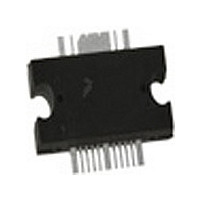
IC PWR AMP RF 26V 20W TO-272-16
Manufacturer
Freescale Semiconductor
Type
Power Amplifierr
Datasheet
1.MW4IC2020GNBR1.pdf
(16 pages)
Specifications of MW4IC2020NBR1
Current - Supply
80mA
Frequency
1.6GHz ~ 2.4GHz
Gain
29dB
Package / Case
TO-272-16
Rf Type
Cellular, GSM, EDGE, CDMA
Voltage - Supply
26V
Number Of Channels
1
Power Supply Requirement
Single
Single Supply Voltage (min)
26V
Single Supply Voltage (max)
28V
Dual Supply Voltage (min)
Not RequiredV
Dual Supply Voltage (typ)
Not RequiredV
Dual Supply Voltage (max)
Not RequiredV
Pin Count
16
Mounting
Surface Mount
Lead Free Status / RoHS Status
Lead free / RoHS Compliant
Noise Figure
-
P1db
-
Test Frequency
-
Lead Free Status / Rohs Status
Compliant
Available stocks
Company
Part Number
Manufacturer
Quantity
Price

Part Number:
MW4IC2020NBR1
Manufacturer:
FREESCALE
Quantity:
20 000


2
MW4IC2020NBR1 MW4IC2020GNBR1
Table 1. Maximum Ratings
Table 2. Thermal Characteristics
Table 3. ESD Protection Characteristics
Table 4. Moisture Sensitivity Level
Table 5. Electrical Characteristics
Functional Tests (In Freescale Wideband 1805 - 1990 MHz Test Fixture, 50 ohm system) V
I
Typical Performances (In Freescale Test Fixture, 50 ohm system) V
1805 MHz<Frequency<1990 MHz, 1 - Tone
DQ3
Drain- Source Voltage
Gate- Source Voltage
Storage Temperature Range
Operating Junction Temperature
Input Power
Thermal Resistance, Junction to Case
Human Body Model
Machine Model
Charge Device Model
Per JESD 22 - A113, IPC/JEDEC J - STD - 020
Power Gain
Drain Efficiency
Input Return Loss
Intermodulation Distortion
Saturated Pulsed Output Power
Quiescent Current Accuracy over Temperature ( - 10 to 85°C)
Gain Flatness in 30 MHz Bandwidth @ P
Deviation from Linear Phase in 30 MHz Bandwidth @ P
Delay @ P
Part - to - Part Phase Variation @ P
1. Refer to AN1955, Thermal Measurement Methodology of RF Power Amplifiers. Go to http://www.freescale.com/rf.
2. Refer to AN1977, Quiescent Current Thermal Tracking Circuit in the RF Integrated Circuit Family. Go to http://www.freescale.com/rf. Select
(f = 1 kHz, Duty Cycle 10%)
= 300 mA, P
Select Documentation/Application Notes - AN1955.
Documentation/Application Notes - AN1977.
out
= 1 W CW Including Output Matching
out
= 20 W PEP, f1 = 1990 MHz, f2 = 1990.1 MHz and f1 = 1805 MHz, f2 = 1805.1 MHz, Two - Tone CW
Test Methodology
Characteristic
Test Conditions
Characteristic
out
f1 = 1805 MHz, f2 = 1805.1 MHz
f1 = 1990 MHz, f2 = 1990.1 MHz
Rating
= 1 W CW
(T
out
C
= 25°C unless otherwise noted)
= 1 W CW
1805- 1880 MHz
1930- 1990 MHz
out
Stage 1
Stage 2
Stage 3
= 1 W CW
(2)
DD
= 26 Vdc, I
Rating
3
Symbol
Delay
ΔI
IMD
P
G
IRL
ΦΔ
η
G
Φ
sat
QT
ps
D
DQ1
F
= 80 mA, I
Symbol
Symbol
V
R
V
T
P
DD
DSS
T
Package Peak Temperature
θJC
GS
stg
in
J
Min
= 26 Vdc, I
27
24
18
—
—
—
—
—
—
—
—
DQ2
= 200 mA, I
260
DQ1
M3 (Minimum)
C5 (Minimum)
2 (Minimum)
0.15
±0.5
±0.2
Typ
±10
- 32
1.8
29
26
20
33
±5
—
- 65 to +175
= 80 mA, I
Class
- 0.5, +65
- 0.5, +15
Value
Value
10.5
200
5.1
2.3
20
Freescale Semiconductor
DQ3
(1)
= 300 mA,
DQ2
Max
- 10
- 27
—
—
—
—
—
—
—
—
RF Device Data
= 200 mA,
(continued)
°C/W
Unit
Unit
dBm
Unit
Vdc
Vdc
Unit
°C
dBc
°C
°C
dB
dB
dB
ns
W
%
%
°
°
Related parts for MW4IC2020NBR1
Image
Part Number
Description
Manufacturer
Datasheet
Request
R

Part Number:
Description:
Manufacturer:
Freescale Semiconductor, Inc
Datasheet:
Part Number:
Description:
Manufacturer:
Freescale Semiconductor, Inc
Datasheet:
Part Number:
Description:
Manufacturer:
Freescale Semiconductor, Inc
Datasheet:
Part Number:
Description:
Manufacturer:
Freescale Semiconductor, Inc
Datasheet:
Part Number:
Description:
Manufacturer:
Freescale Semiconductor, Inc
Datasheet:
Part Number:
Description:
Manufacturer:
Freescale Semiconductor, Inc
Datasheet:
Part Number:
Description:
Manufacturer:
Freescale Semiconductor, Inc
Datasheet:
Part Number:
Description:
Manufacturer:
Freescale Semiconductor, Inc
Datasheet:
Part Number:
Description:
Manufacturer:
Freescale Semiconductor, Inc
Datasheet:
Part Number:
Description:
Manufacturer:
Freescale Semiconductor, Inc
Datasheet:
Part Number:
Description:
Manufacturer:
Freescale Semiconductor, Inc
Datasheet:
Part Number:
Description:
Manufacturer:
Freescale Semiconductor, Inc
Datasheet:
Part Number:
Description:
Manufacturer:
Freescale Semiconductor, Inc
Datasheet:
Part Number:
Description:
Manufacturer:
Freescale Semiconductor, Inc
Datasheet:
Part Number:
Description:
Manufacturer:
Freescale Semiconductor, Inc
Datasheet: