WS2111-TR1 Avago Technologies US Inc., WS2111-TR1 Datasheet
WS2111-TR1
Specifications of WS2111-TR1
Available stocks


Related parts for WS2111-TR1


WS2111-TR1 Summary of contents
Page 1
... Description The WS2111, a Wide-band Code Division Multiple Access (WCDMA) Power Amplifier (PA fully matched 10-pin surface mount module developed for WCDMA handset applications. This power amplifier module operates in the 824–849 MHz bandwidth. The WS2111 meets the stringent WCDMA linearity requirements for output power dBm ...
Page 2
Table 1. Absolute Maximum Ratings [1] Parameter Symbol RF Input Power Supply Voltage Reference Voltage V ref Storage Temperature T stg Table 2. Recommended Operating Conditions Parameter Symbol DC Supply Voltage – Mid/High Power ...
Page 3
Electrical Specifications Table 4. Electrical Characteristics for WCDMA Mode (Vcc=3.4V, Vref=2.85V, Temp=+25°C) Characteristics Operating Frequency Range Gain Power Added Efficiency Total Supply Current Quiescent Current Reference Current Control Current [3] Total Current in Power-down mode ACLR in High power mode ...
Page 4
Table 4. Electrical Characteristics for WCDMA Mode (Vcc=3.4V, Vref=2.85V, Temp=+25°C) continued Characteristics Switching Time High [ Switching Time Low [ Turn On Time [ Turn Off Time DC [6] RF Notes: 5. TswhighDC, TswlowDC ...
Page 5
Characterization Data ( HSDPA, Control scheme: 3-mode control, Vcc = 3.4V, Vref = 2.85V 25° 837 MHz) 500 450 400 350 300 250 200 150 100 Pout (dBm) ...
Page 6
Characterization Data (WCDMA, Control scheme: 3-mode control, Vcc = 3.4V, Vref = 2.85V 25° 837 MHz) 500 450 400 350 300 250 200 150 100 Pout (dBm) Figure ...
Page 7
Characterization Data (WCDMA, Control scheme: 2-mode control, Vcc = 3.4V, Vref = 2.85V 25° 837 MHz) 500 450 400 350 300 250 200 150 100 Pout (dBm) Figure ...
Page 8
... Vref 1 Vref C4 Vcont 100pF 2 Vcont C3 R1 100pF 6.2kohm 3 GND Vcc1 C1 C5 Vcc1 470pF 2.2µF Figure 17. Evaluation Board Schematic Agilent WS2111 PYYWW AAAAA ` C1 C5 Figure 18. Evaluation Board Assembly Diagram. 8 GND 10 GND 9 RF Out 8 GND 7 Vcc2 6 C2 470pF Out Vcc2 C6 2.2µF ...
Page 9
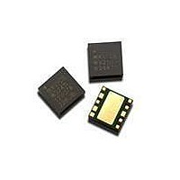
Package Dimensions and Pin Descriptions Pin 1 Mark ± 0.05 TOP VIEW 1.9 1.0 0.5 0.85 0.6 0.85 1.7 1.9 BOTTOM VIEW all dimensions are in millimeters Figure 19. Package Dimensional Drawing and Pin ...
Page 10
... Package Dimensions and Pin Descriptions, continued Pin 1 Mark Agilent WS2111 PYYWW AAAAA Figure 20. Marking Specification. 10 Manufacturing Part Number Lot Number P Manufacturing Site YY Manufacturing Year WW Work Week AAAAA Assembly Lot Number ...
Page 11
... Place C3 and C4 close to pin 5 (Vcc1) and pin 6 (Vcc2). These capacitors can affect the RF performance. 4. Use 50Ω transmission line between PAM and Duplexer and make it as short as possible to reduce conduction loss. 5. π-type circuit topology is good to use for matching circuit between PA and Duplexer,. 6. Pull-up resistor (R1) should be used to limit current drain. 6.2 kohm is recommended for WS2111 ...
Page 12
... Probability Distribution Function implies that what is important for longer talk time is the effi- ciency of low or medium power range rather than the efficiency at full power. WS2111 idle current and operating current at 16 dBm nominal condition. Average current calculated with CDMA PDF urban area and suburban area for 2- mode control ...
Page 13
... PCB Design Guidelines The recommended WS2111 PCB Land pattern is shown in Figure 25 and Figure 26. The substrate is coated with solder mask between the I/O and conductive paddle to protect the gold pads from short circuit that is caused by solder bleeding/bridging. Stencil Design Guidelines A properly designed solder ...
Page 14
... PAE graphs for 2-mode control and 3-mode control are shown in Figure 28 and Figure 29. HSDPA WS2111 meets stringent HSDPA linearity requirement up to 27.5 dBm. WS2111 can operate dBm with Rel.99, which has a lower PAR (peak-to-average ratio) than HSDPA ...
Page 15
... Ordering Information Part Number Number of Devices WS2111-BLK 100 WS2111-TR1 2500 Tape and Reel Information Dimension List Annote Millimeter 4.40 ± 0.10 A0 4.40 ± 0.10 B0 1.70 ± 0.10 K0 1.55 ± 0.05 D0 1.60 ± 0.10 D1 4.00 ± 0.10 P0 8.00 ± 0.10 P1 all dimensions are in millimeters Figure 30. Tape and Reel Format – ...
Page 16
Tape and Reel Information, continued all dimensions are in millimeters Figure 31. Plastic Reel Format –13"/14". 16 ...
Page 17
... After this time period, the part would need to be removed from the reel, de-taped and then re-baked. MSL classification reflow temperature for the WS2111 is targeted at 250° C +0/-5° C. Figure 32 and Table 9 show typical SMT profile for maximum tempera- ture of 250+0/-5° C. ...
Page 18
Handling and Storage, continued Figure 32. Typical SMT Reflow Profile for Maximum Temperature = 250+0/-5°C. Table 9. Typical SMT Reflow Profile for Maximum Temperature = 250+0/-5°C Profile Feature Average ramp-up rate ( Preheat - Temperature ...
Page 19
Handling and Storage, continued Storage Conditions Packages described in this document must be stored in sealed moisture barrier, anti- static bags. Shelf life in a sealed moisture barrier bag months at <40 C and 90% relative humidity ...
Page 20
Handling and Storage, continued Table 10. Recommended Equivalent Total Floor Life (days) @ 20°C, 25°C & 30°C For ICs with Novolac, Biphenyl and Multifunctional Epoxies (Reflow at same temperature at which the component was classified) www.agilent.com/semiconductors For product information and ...