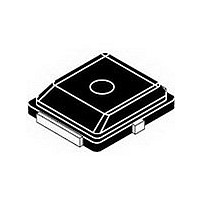
MW4IC001MR4 Freescale Semiconductor, MW4IC001MR4 Datasheet

MW4IC001MR4
Specifications of MW4IC001MR4
Related parts for MW4IC001MR4
MW4IC001MR4 Summary of contents
Page 1
... MHz, 900 mW INTEGRATED POWER AMPLIFIER = Symbol V DSS stg T J Symbol R θJC Rating Package Peak Temperature 3 MW4IC001MR4 Rev. 4, 5/2006 W - CDMA RF LDMOS WIDEBAND CASE 466 - 03, STYLE 1 PLD - 1.5 PLASTIC Value Unit - 0.5, +65 Vdc - 0.5, +15 Vdc 4.58 W 0.037 W/° +150 °C 150 °C ...
Page 2
... MW4IC001MR4 Unit μAdc μAdc μAdc Vdc Vdc Vdc dBc ...
Page 3
... Microstrip Z6, Z7 1.915″ x 0.055″ Microstrip Z8 0.120″ x 0.141″ Microstrip Figure 1. MW4IC001MR4 900 MHz Test Circuit Schematic Table 6. MW4IC001MR4 900 MHz Test Circuit Component Designations and Values Part C1, C6 0.1 μF, 100 V Chip Capacitors C2, C3, C5 pF, 500 V Chip Capacitors ...
Page 4
... Freescale has begun the transition of marking Printed Circuit Boards (PCBs) with the Freescale Semiconductor signature/logo. PCBs may have either Motorola or Freescale markings during the transition period. These changes will have no impact on form, fit or function of the current product. Figure 2. MW4IC001MR4 900 MHz Test Circuit Component Layout RF Device Data Freescale Semiconductor ...
Page 5
... Order −60 Two −Tone Measurement −65 100 kHz Tone Spacing 7th Order −70 0.01 0 OUTPUT POWER (WATTS) PEP out Figure 6. Intermodulation Distortion Products versus Output Power MW4IC001MR4 16 TYPICAL CHARACTERISTICS - 900 MHz IRL η Vdc 0.9 W (PEP) out Two −Tone Measurement ...
Page 6
... Microstrip Z7 0.076″ x 0.150″ Microstrip Z8 0.294″ x 0.150″ Microstrip Figure 8. MW4IC001MR4 1990 MHz Test Circuit Schematic Table 7. MW4IC001MR4 1990 MHz Test Circuit Component Designations and Values Part C1 μ Tantalum Capacitors C2 pF, 500 V Chip Capacitors C3, C5 ...
Page 7
... mA 1990 MHz 1990.1 MHz −70 DQ Two−Tone Measurement, 100 kHz Tone Spacing −75 0.01 0.1 OUTPUT POWER (WATTS) PEP Figure 13. Intermodulation Distortion Products versus Output Power MW4IC001MR4 18 TYPICAL CHARACTERISTICS - 1990 MHz IRL η Vdc 0.9 W (PEP out DQ Two−Tone Measurement, 100 kHz Tone Spacing ...
Page 8
... Microstrip Z7 0.109″ x 0.150″ Microstrip Z8 0.210″ x 0.150″ Microstrip Figure 15. MW4IC001MR4 2170 MHz Test Circuit Schematic Table 8. MW4IC001MR4 2170 MHz Test Circuit Component Designations and Values Part C1 μ Tantalum Capacitors C2 pF, 500 V Chip Capacitors C3, C5 ...
Page 9
... Order −40 −45 −50 5th Order −55 −60 7th Order −65 −70 0.01 0 OUTPUT POWER (WATTS) PEP out Figure 20. Intermodulation Distortion Products versus Output Power MW4IC001MR4 Vdc 0.9 W (PEP) out Two−Tone Measurement, 100 kHz Tone Spacing ps 2120 2130 2140 ...
Page 10
... Z = Test circuit impedance as measured from source gate to ground Test circuit impedance as measured load from drain to ground. Device Input Matching Under Test Network Z Z source load f = 860 MHz 900 MHz load Ω o Output Matching Network MW4IC001MR4 21 ...
Page 11
... Z = Test circuit impedance as measured load from drain to ground. Input Device Matching Under Test Network Z Z source load Figure 23. Series Equivalent Source and Load Impedance MW4IC001MR4 22 Z load f = 2000 MHz Z load MHz Ω 2100 2110 2120 2130 2140 2150 2160 ...
Page 12
... RF Device Data Freescale Semiconductor NOTES MW4IC001MR4 23 ...
Page 13
... MW4IC001MR4 24 NOTES RF Device Data Freescale Semiconductor ...
Page 14
... RF Device Data Freescale Semiconductor NOTES MW4IC001MR4 25 ...
Page 15
... ZONE W 1 É É É É É É É É É É É É É É É É É É É É É ZONE X VIEW MW4IC001MR4 26 PACKAGE DIMENSIONS " 0.35 (0.89 STYLE 1: PIN 1 ...
Page 16
... Freescale Semiconductor was negligent regarding the design or manufacture of the part. Freescalet and the Freescale logo are trademarks of Freescale Semiconductor, Inc. All other product or service names are the property of their respective owners. © Freescale Semiconductor, Inc. 2006. All rights reserved. MW4IC001MR4 27 ...


