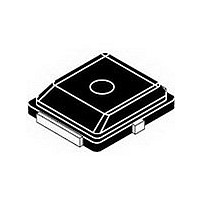
MW4IC001NR4 Freescale Semiconductor, MW4IC001NR4 Datasheet

MW4IC001NR4
Specifications of MW4IC001NR4
Related parts for MW4IC001NR4
MW4IC001NR4 Summary of contents
Page 1
... Freescale Semiconductor Technical Data Replaced by MW4IC001NR4. There are no form, fit or function changes with this part replacement. N suffix added to part number to indicate transition to lead - free terminations. RF LDMOS Wideband Integrated Power Amplifier The MW4IC001M wideband integrated circuit is designed for use as a distortion signature device in analog predistortion systems. It uses Freescale’s newest High Voltage ( Volts) LDMOS IC technology ...
Page 2
... DQ Common - Source Amplifier Power Gain ( Vdc 0 out DQ Drain Efficiency ( Vdc 0 out DQ Input Return Loss ( Vdc 0 out DQ RF Device Data Freescale Semiconductor = 25°C unless otherwise noted) C Symbol I DSS I DSS I GSS V GS(th) V GS(Q) V DS(on oss = 0 Vdc rss ...
Page 3
... T491X226K035AS 100B4R7CP500X 27271SL 100B2R7CP500X 100B3R3CP500X 0805 Series 1008 Series CRCW12061001F100 CRCW120620R0F100 OUTPUT Z10 Z11 Z12 Z13 C5 C11 C13 C12 = 3.5 r Part Number Manufacturer Kemet ATC ATC Kemet ATC Johanson ATC ATC AVX ATC Dale Dale RF Device Data Freescale Semiconductor ...
Page 4
... MW4IC001MR4 900 MHz Rev 2 Freescale has begun the transition of marking Printed Circuit Boards (PCBs) with the Freescale Semiconductor signature/logo. PCBs may have either Motorola or Freescale markings during the transition period. These changes will have no impact on form, fit or function of the current product. ...
Page 5
... OUTPUT POWER (WATTS) PEP out Figure 5. Intermodulation Distortion versus Output Power Vdc DS 10 MHz MHz f1 = 880 MHz Tone Spacing Two −Tone Measurement 0 OUTPUT POWER (WATTS) PEP out Figure 7. Third Order Intermodulation Distortion versus Output Power RF Device Data Freescale Semiconductor = 28 Vdc 10 10 ...
Page 6
... MW4IC001MR4 1990 MHz Rev 3 Freescale has begun the transition of marking Printed Circuit Boards (PCBs) with the Freescale Semiconductor signature/logo. PCBs may have either Motorola or Freescale markings during the transition period. These changes will have no impact on form, fit or function of the current product. ...
Page 7
... Tone Spacing 0 OUTPUT POWER (WATTS) PEP out Figure 12. Intermodulation Distortion versus Output Power 10 MHz 1 MHz Vdc 1990 MHz Tone Spacing 100 kHz Two −Tone Measurement 0 OUTPUT POWER (WATTS) PEP out Figure 14. Third Order Intermodulation Distortion versus Output Power RF Device Data Freescale Semiconductor 1 1 ...
Page 8
... MW4IC001MR4 2170 MHz Rev 3 Freescale has begun the transition of marking Printed Circuit Boards (PCBs) with the Freescale Semiconductor signature/logo. PCBs may have either Motorola or Freescale markings during the transition period. These changes will have no impact on form, fit or function of the current product. ...
Page 9
... MHz −40 −45 1 0.01 Figure 21. Third Order Intermodulation −13 −18 −23 −28 −33 2170 OUTPUT POWER (WATTS) PEP out Output Power = 28 Vdc 10 MHz 100 kHz 0 OUTPUT POWER (WATTS) PEP out Distortion versus Output Power RF Device Data Freescale Semiconductor 1 1 ...
Page 10
... Figure 22. Series Equivalent Source and Load Impedance RF Device Data Freescale Semiconductor Z source f = 900 MHz f =860 MHz mA 0.9 W PEP DD DQ out source load MHz Ω Ω 860 27.853 + j5.908 15.492 + j63.669 15.592 + j68.687 865 28.617 + j6.078 870 29.458 + j6.285 15.788 + j69.799 875 30 ...
Page 11
... Test circuit impedance as measured from gate to ground. = Test circuit impedance as measured from drain to ground. Output Device Matching Under Test Network Z Z source load RF Device Data Freescale Semiconductor ...
Page 12
... RF Device Data Freescale Semiconductor NOTES MW4IC001MR4 23 ...
Page 13
... MW4IC001MR4 24 NOTES RF Device Data Freescale Semiconductor ...
Page 14
... RF Device Data Freescale Semiconductor NOTES MW4IC001MR4 25 ...
Page 15
... P 0.000 0.008 0.00 0.20 Q 0.055 0.063 1.40 1.60 R 0.200 0.210 5.08 5.33 S 0.006 0.012 0.15 0.31 U 0.006 0.012 0.15 0.31 ZONE V 0.000 0.021 0.00 0.53 ZONE W 0.000 0.010 0.00 0.25 ZONE X 0.000 0.010 0.00 0.25 RF Device Data Freescale Semiconductor ...
Page 16
... Freescale Semiconductor product could create a situation where personal injury or death may occur. Should Buyer ...


