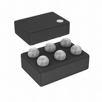
AD8312ACBZ-P7 Analog Devices Inc, AD8312ACBZ-P7 Datasheet

AD8312ACBZ-P7
Specifications of AD8312ACBZ-P7
AD8312ACBZ-P7TR
Available stocks
Related parts for AD8312ACBZ-P7
AD8312ACBZ-P7 Summary of contents
Page 1
FEATURES Complete RF detector function Typical range: −45 dBm to 0 dBm Ω Frequency response from 50 MHz to 3.5 GHz Temperature-stable linear-in-dB response Accurate to 3.5 GHz Rapid response: 85/120 ns (rise/fall) Low power ...
Page 2
AD8312 TABLE OF CONTENTS Specifications ..................................................................................... 3 Absolute Maximum Ratings ............................................................ 6 ESD Caution .................................................................................. 6 Pin Configuration and Function Descriptions ............................. 7 Typical Performance Characteristics ............................................. 8 General Description ....................................................................... 12 Applications ..................................................................................... 13 Basic Connections ...................................................................... 13 Transfer ...
Page 3
SPECIFICATIONS CFLT = open 25°C, light condition = 600 LUX, 52.3 Ω termination resistor at RFIN, unless otherwise noted Table 1. Parameter Conditions SIGNAL INPUT INTERFACE RFIN (Pin 6) Specified Frequency Range ...
Page 4
AD8312 Parameter Conditions f = 1.9 GHz Input Impedance ±1 dB Dynamic Range T −40°C < T Maximum Input Level ±1 dB error Minimum Input Level ±1 dB error Slope Intercept Output Voltage − High Power In P Output Voltage ...
Page 5
Parameter Conditions POWER INTERFACE VPOS (Pin 1) Supply Voltage Quiescent Current vs. Temperature −40°C ≤ Increased output is possible when using an attenuator between VOUT and VSET to raise the slope. ≤ +85°C A Rev Page ...
Page 6
AD8312 ABSOLUTE MAXIMUM RATINGS Table 2. Parameter Supply Voltage VPOS VOUT, VSET Input Voltage Equivalent Power Internal Power Dissipation θ (WLCSP) JA Maximum Junction Temperature Operating Temperature Range Storage Temperature Range ESD CAUTION ESD (electrostatic discharge) sensitive device. Electrostatic charges ...
Page 7
PIN CONFIGURATION AND FUNCTION DESCRIPTIONS Table 3. Pin Function Descriptions Ball No. Mnemonic Description 1 VPOS Positive Supply Voltage (V 2 VOUT Logarithmic Output. Output voltage increases with increasing input amplitude. 3 VSET Setpoint Input. Connect VSET to VOUT for ...
Page 8
AD8312 TYPICAL PERFORMANCE CHARACTERISTICS 25° open; light condition = 600 LUX, 52.3 Ω termination; unless otherwise noted. Colors: +25°C = Black FLT −40°C = Blue, +85°C = Red. 1.25 +85°C ...
Page 9
P (dBm) IN Figure 9. Distribution of Error at −40°C, +25°C, and +85°C After Ambient Normalization vs. Input Amplitude at 50 ...
Page 10
AD8312 100ns/HORIZ DIV RISE TIME 85ns 500mV/ VERT DIV VOUT PULSED RF 0.1GHz, 0dBm RF INPUT 200mV/VERT DIV Figure 15. VOUT Response Time, RF Off to 0 dBm ROHDE & SCHWARZ TRIG OUT SMT06 GENERATOR PULSE MODULATION RF OUT +3dB ...
Page 11
Table 4. Typical Specifications at Selected Frequencies at 25°C (Mean and Σ) Slope (mV/dB) μ Frequency (GHz) 0.05 20.25 0.1 21.0 0.9 20.25 1.9 19.47 2.2 19.1 2.5 18.6 3.0 17.5 3.5 17.1 1 Refer to Figure 23. Intercept (dBm) ...
Page 12
AD8312 GENERAL DESCRIPTION The AD8312 is a logarithmic amplifier (log amp) similar in design to the AD8313; further details about the structure and function may be found in the AD8313 data sheet and the data sheets of other log amplifiers ...
Page 13
APPLICATIONS BASIC CONNECTIONS Figure 22 shows the basic connections for measurement mode. A supply voltage required. The supply to the VPOS pin should be decoupled with a low inductance 0.1 μF surface-mount ceramic ...
Page 14
AD8312 Filter Capacitor The video bandwidth of VOUT is approximately 3.5 MHz applications where the input frequency is much higher than this, no further filtering of the demodulated signal is required. Where there is a low frequency modulation ...
Page 15
Table 5. Input Impedance for Select Frequency Frequency S11 (GHz) Real Imaginary 0.05 0.967 −0.043 0.1 0.962 −0.081 0.9 0.728 −0.535 1.9 0.322 −0.891 2.2 0.230 −0.832 2.5 0.165 −0.845 3.0 0.126 −0.849 3.5 0.146 −0.826 Increasing the Logarithmic Slope ...
Page 16
AD8312 IS-95 REV 0 –1 –2 –3 WCDMA 64-CH 64 QAM –4 –5 –60 –50 –40 –30 –20 INPUT (dBm) Figure 29. Shift in Transfer Function due to Several Different Signal Waveforms Temperature Drift ...
Page 17
VOUT R8 C4 (OPEN) (OPEN) R7 0Ω CONNECTOR VSET R2 R5 (OPEN) (OPEN) TO EDGE CONNECTOR Figure 34. Silkscreen of Component Side (WLCSP) Figure 35. Layout of Component Side (WLCSP) C2 0.1μF AD8312 VPOS VPOS RFIN 1 R3 0Ω VOUT ...
Page 18
AD8312 Table 6. Evaluation Board Configuration Options Component Function VPOS, GND Supply and Ground Vector Pins. C2 Power Supply Decoupling. The nominal supply decoupling consists of a 0.1 μF capacitor (C1). R1 Input Interface. The 52.3 Ω resistor in Position ...
Page 19
... OUTLINE DIMENSIONS A1 BALL CORNER TOP VIEW (BALL SIDE DOWN) ORDERING GUIDE Model 1 Temperature Range AD8312ACBZ-P7 –40°C to +85°C AD8312ACBZ-P2 –40°C to +85°C AD8312-EVALZ RoHS Compliant Part. 0.675 0.595 0.380 1.00 0.515 0.355 0.95 SEATING 0.330 0.90 PLANE 0.345 0.295 1 ...
Page 20
AD8312 NOTES ©2005–2011 Analog Devices, Inc. All rights reserved. Trademarks and registered trademarks are the property of their respective owners. D05260–0–1/11(A) Rev Page ...


