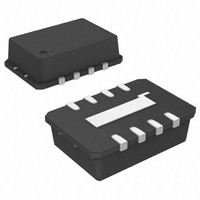
AD8319ACPZ-R7 Analog Devices Inc, AD8319ACPZ-R7 Datasheet

AD8319ACPZ-R7
Specifications of AD8319ACPZ-R7
Related parts for AD8319ACPZ-R7
AD8319ACPZ-R7 Summary of contents
Page 1
FEATURES Wide bandwidth: 1 MHz to 10 GHz High accuracy: ±1.0 dB over temperature 45 dB dynamic range GHz Stability over temperature: ±0.5 dB Low noise measurement/controller output VOUT Pulse response time (fall/rise): 6 ns/10 ns Small ...
Page 2
AD8319 TABLE OF CONTENTS Features .............................................................................................. 1 Applications....................................................................................... 1 Functional Block Diagram .............................................................. 1 General Description ......................................................................... 1 Revision History ............................................................................... 2 Specifications..................................................................................... 3 Absolute Maximum Ratings............................................................ 5 ESD Caution.................................................................................. 5 Pin Configuration and Function Descriptions............................. 6 Typical Performance Characteristics ...
Page 3
SPECIFICATIONS 1000 pF 25°C, 52.3 Ω termination resistor at INHI, unless otherwise noted. POS LPF A Table 1. Parameter SIGNAL INPUT INTERFACE Specified Frequency Range DC Common-Mode Voltage MEASUREMENT MODE f = ...
Page 4
AD8319 Parameter f = 5.8 GHz Input Impedance ±1 dB Dynamic Range Maximum Input Level Minimum Input Level 1 Slope 1 Intercept Output Voltage: High Power In Output Voltage: Low Power 8.0 GHz Input Impedance ±1 dB ...
Page 5
ABSOLUTE MAXIMUM RATINGS Table 2. Parameter Supply Voltage: V POS V Voltage SET Input Power (Single-Ended, re: 50 Ω) Internal Power Dissipation θ JA Maximum Junction Temperature Operating Temperature Range Storage Temperature Range Lead Temperature (Soldering, 60 sec) Stresses above ...
Page 6
AD8319 PIN CONFIGURATION AND FUNCTION DESCRIPTIONS Table 3. Pin Function Descriptions Pin No. Mnemonic Description 1 INHI RF Input. Nominal input range of −50 dBm to 0 dBm, re: 50 Ω; ac-coupled RF input. 2 COMM Device Common. Connect this ...
Page 7
TYPICAL PERFORMANCE CHARACTERISTICS 25°C, −40°C, +85°C; C POS LPF using the best fit line between P = −40 dBm and P IN 2.00 1.75 1.50 1.25 1.00 0.75 0.50 0.25 0 –60 –50 –40 ...
Page 8
AD8319 2.00 1.75 1.50 1.25 1.00 0.75 0.50 0.25 0 –60 –50 –40 –30 –20 P (dBm) IN Figure 9. V and Log Conformance Error vs. Input Amplitude at 900 MHz, OUT Multiple Devices kΩ TADJ 2.00 ...
Page 9
START FREQUENCY = 0.05GHz –j1 STOP FREQUENCY = 10GHz 10000MHz 5800MHz Figure 15. Input Impedance vs. Frequency; No Termination Resistor on INHI (Impedance De-Embedded to Input Pins ...
Page 10
AD8319 THEORY OF OPERATION The AD8319 is a five-stage demodulating logarithmic amplifier, specifically designed for use in RF measurement and power control applications at frequencies GHz. A block diagram is shown in Figure 21. Sharing much of ...
Page 11
USING THE AD8319 BASIC CONNECTIONS The AD8319 is specified for operation GHz result, low impedance supply pins with adequate isolation between functions are essential. A power supply voltage of between 3.0 V and 5.5 V ...
Page 12
AD8319 The slope is given by −I × 2x × 1.5 kΩ = −22 mV/dB × x. For D example resistor divider to ground is used to generate a V voltage The ...
Page 13
For example, P for a sinusoidal input signal expressed in INTERCEPT terms of dBm (decibels referred Ω system is P (dBm) = INTERCEPT P (dBV) − 10 × log (Z × 1 mW/1 V ...
Page 14
AD8319 RF INPUT SIGNAL Figure 30. AD8319 Operating in Controller Mode to Provide Automatic Gain Control Functionality in Combination with the ADL5330 The basic connections for operating the AD8319 in an automatic gain control (AGC) loop with the ADL5330 Figure ...
Page 15
For the AGC loop to remain in equilibrium, the AD8319 must track the envelope of the output signal of the provide the necessary voltage levels to the gain control input of the ADL5330. Figure 32 shows an oscilloscope screenshot of ...
Page 16
AD8319 OPERATION BEYOND 8 GHz The AD8319 is specified for operation GHz, but it provides useful measurement accuracy over a reduced dynamic range GHz. Figure 35 shows the performance of the AD8319 over ...
Page 17
EVALUATION BOARD R1 52.3Ω RFIN Table 5. Evaluation Board (Rev. A) Configuration Options Component Function VPOS, GND Supply and Ground Connections. R1, C1, C2 Input Interface. The 52.3 Ω resistor in Position R1 combines with the internal input impedance of ...
Page 18
AD8319 Figure 37. Component Side Layout Figure 38. Component Side Silkscreen Rev Page ...
Page 19
... OUTLINE DIMENSIONS 1.95 1.75 1.55 PIN 1 INDICATOR 12° MAX 1.00 0.85 0.80 SEATING PLANE ORDERING GUIDE Model Temperature Range 1 AD8319ACPZ-R7 –40°C to +85°C 1 AD8319ACPZ-R2 –40°C to +85°C 1 AD8319ACPZ-WP –40°C to +85°C 1 AD8319-EVALZ RoHS Compliant Part. 3.25 3.00 0.55 2.75 ...
Page 20
AD8319 NOTES ©2005–2008 Analog Devices, Inc. All rights reserved. Trademarks and registered trademarks are the property of their respective owners. D05705-0-4/08(B) Rev Page ...


