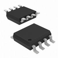
AD8313ARM Analog Devices Inc, AD8313ARM Datasheet - Page 13

AD8313ARM
Manufacturer Part Number
AD8313ARM
Description
IC LOGARTIHMIC AMP 70DB 8-MSOP
Manufacturer
Analog Devices Inc
Type
Logarithmic Ampr
Datasheet
1.AD8313ARMZ.pdf
(24 pages)
Specifications of AD8313ARM
Rohs Status
RoHS non-compliant
Frequency
100MHz ~ 2.5GHz
Rf Type
RADAR, 802.11/Wi-Fi, 8.2.16/WiMax, Wireless LAN
Input Range
-65dBm ~ 0dBm
Accuracy
±1dB
Voltage - Supply
2.7 V ~ 5.5 V
Current - Supply
13.7mA
Package / Case
8-TSSOP, 8-MSOP (0.118", 3.00mm Width)
Number Of Channels
1
Number Of Elements
8
Power Supply Requirement
Single
Voltage Gain Db
84dB
Input Resistance
0.0009@5VMohm
Input Bias Current
10@5VnA
Single Supply Voltage (typ)
3/5V
Dual Supply Voltage (typ)
Not RequiredV
Power Dissipation
200mW
Rail/rail I/o Type
Rail to Rail Output
Single Supply Voltage (min)
2.7V
Single Supply Voltage (max)
5.5V
Dual Supply Voltage (min)
Not RequiredV
Dual Supply Voltage (max)
Not RequiredV
Operating Temp Range
-40C to 85C
Operating Temperature Classification
Industrial
Mounting
Surface Mount
Pin Count
8
Package Type
MSOP
Lead Free Status / RoHS Status
Not Compliant
Available stocks
Company
Part Number
Manufacturer
Quantity
Price
Company:
Part Number:
AD8313ARM
Manufacturer:
AD
Quantity:
5 510
Company:
Part Number:
AD8313ARM
Manufacturer:
NAIS
Quantity:
5 510
Company:
Part Number:
AD8313ARM
Manufacturer:
AD
Quantity:
4 130
Part Number:
AD8313ARM
Manufacturer:
ADI/亚德诺
Quantity:
20 000
Company:
Part Number:
AD8313ARM-REEL
Manufacturer:
AD
Quantity:
5 510
Company:
Part Number:
AD8313ARM-REEL
Manufacturer:
LT
Quantity:
5 510
Part Number:
AD8313ARM-REEL
Manufacturer:
ADI/亚德诺
Quantity:
20 000
Part Number:
AD8313ARM-REEL7
Manufacturer:
ADI/亚德诺
Quantity:
20 000
Part Number:
AD8313ARMZ
Manufacturer:
ADI/亚德诺
Quantity:
20 000
Part Number:
AD8313ARMZ-REEL
Manufacturer:
ADI/亚德诺
Quantity:
20 000
INTERFACES
This section describes the signal and control interfaces and
their behavior. On-chip resistances and capacitances exhibit
variations of up to ±20%. These resistances are sometimes
temperature-dependent, and the capacitances may be voltage-
dependent.
POWER-DOWN INTERFACE, PWDN
The power-down threshold is accurately centered at the
midpoint of the supply as shown in Figure 24. If Pin 5 is left
unconnected or tied to the supply voltage (recommended), the
bias enable current is shut off, and the current drawn from the
supply is predominately through a nominal 300 kΩ chain
(20 µA at 3 V). When grounded, the bias system is turned on.
The threshold level is accurately at V
the device ON state, the input bias current at the PWDN pin is
approximately 5 µA for V
SIGNAL INPUTS, INHI, INLO
The simplest low frequency ac model for this interface consists
of just a 900 Ω resistance, R
acitance, C
these distributed in the context of a more complete schematic.
The input bias voltage shown is for the enabled chip; when
disabled, it rises by a few hundred millivolts. If the input is
coupled via capacitors, this change may cause a low level signal
transient to be introduced, having a time constant formed by
these capacitors and R
should be well matched. This is not necessary when using the
small capacitors found in many impedance transforming
networks used at high frequencies.
VPOS
VPOS
INLO
INHI
0.5pF
0.5pF
2
3
4
1
COMM
PWDN
VPOS
IN
, connected across INHI and INLO. Figure 25 shows
Figure 25. Input Interface Simplified Schematic
Figure 24. Power-Down Threshold Circuitry
4
5
6
2.5kΩ
75kΩ
(1ST DETECTOR)
IN
2.5kΩ
. For this reason, large coupling capacitors
1.25kΩ
~
0.75V
POS
0.7pF
IN
= 3 V.
, in shunt with a 1.1 pF input cap-
50kΩ
250Ω
125Ω
POS
/2. When operating in
~
1.4mA
150kΩ
150k Ω
125Ω
GAIN BIAS
1.25kΩ
ENABLE
TO BIAS
1.24V
TO STAGES
1 TO 4
TO 2ND
STAGE
COMM
Rev. D | Page 13 of 24
For high frequency use, Figure 26 shows the input impedance
plotted on a Smith chart. This measured result of a typical
device includes a 191 mil 50 Ω trace and a 680 pF capacitor to
ground from the INLO pin.
LOGARITHMIC/ERROR OUTPUT, VOUT
The rail-to-rail output interface is shown in Figure 27. V
run from within about 50 mV of ground, to within about 100 mV
of the supply voltage, and is short-circuit safe to either supply.
However, the sourcing load current, I
which is provided by the PNP transistor, typically 400 µA.
Larger load currents can be provided by adding an external NPN
transistor (see the Applications section). The dc open-loop gain
of this amplifier is high, and it may be regarded as an integrator
having a capacitance of 2 pF (C
signal generated by the summed outputs of the nine detector
stages, which is scaled approximately 4.0 µA/dB.
Thus, for midscale RF input of about 3 mV, which is some 40 dB
above the minimum detector output, this current is 160 µA, and
the output changes by 8 V/µs. When VOUT is connected to VSET,
the rise and fall times are approximately 40 ns (for R
The nominal slew rate is 2.5 V/µs. The HF compensation tech-
nique results in stable operation with a large capacitive load, C
though the positive-going slew rate is then limited by I
to 1 V/µs for C
DETECTOR
SETPOINT
OUTPUTS
SUMMED
FROM
Frequency
100MHz
900MHz
1.9GHz
2.5GHz
LP
LM
R
650
55
22
23
L
+ j X
– j 400
– j 135
– j 65
– j 43
= 400 pF.
Figure 27. Output Interface Circuitry
Figure 26. Typical Input Impedance
AD8313 MEASURED
2.5GHz
g
m
STAGE
BIAS
INT
) driven by the current-mode
C
1.9GHz
INT
SOURCE
I
400µA
10mA
MAX
SOURCE
, is limited to that
900MHz
900Ω
100MHz
1
8
6
VPOS
VOUT
COMM
L
AD8313
≥ 10 kΩ ).
SOURCE
OUT
1.1pF
C
L
can
/C
L
L
,


