ATR2406-DEV-BOARD2 Atmel, ATR2406-DEV-BOARD2 Datasheet
ATR2406-DEV-BOARD2
Specifications of ATR2406-DEV-BOARD2


Related parts for ATR2406-DEV-BOARD2


ATR2406-DEV-BOARD2 Summary of contents
Page 1
... FCC CFR47, Part 15, ETSI EN 300 328, EN 300 440 and ARIB STD-T-66 Compliant Radio Links 1. Description The ATR2406 is a single chip RF transceiver intended for applications in the 2.4-GHz ISM band. The QFN32-packaged complete transceiver including image rejec- tion mixer, low IF filter, FM demodulator, RSSI, TX preamplifier, power-ramping generator for external power amplifier, integrated synthesizer, and a fully integrated VCO and TX filter ...
Page 2
... Pinning QFN32 - 5 ATR2406 2 VREG REG_CTRL VS_REG IREF AUX AUX REG REG IR-Mixer BP VCO Divider by 2 GAUSSIAN FILTER PLL CP REF_CLK TX_DATA PU_REG 1 REF_CLK 2 RSSI 3 4 VS_IFD ATR2406 VS_IFA 5 RX-CLOCK IREF LIMITER DEMOD RSSI BUS CTRL LOGIC VTUNE 24 RX_ON RAMP_OUT 20 TX_OUT 19 RX_IN1 18 RX_IN2 ...
Page 3
... TX control input 26 nOLE Open loop enable input 27 PU_TRX RX/TX/PLL/VCO power-up input 28 RX_DATA RX data output 29 TX_DATA TX data input 30 CLOCK 3-wire-bus: Clock input 31 DATA 3-wire-bus: Data input 32 ENABLE 3-wire-bus: Enable input Paddle GND Ground 4779N–ISM–12/08 if internal AUX regulator is not used S ATR2406 3 ...
Page 4
... PC for the phase detector (PD) (f supported. 3.5 Power Supply An integrated band-gap–stabilized voltage regulator for use with an external low-cost PNP tran- sistor is implemented. Multiple power-down and current saving modes are provided. ATR2406 4 = 1.728 MHz). Open loop modulation is PD 4779N–ISM–12/08 ...
Page 5
... Input frequency range 4779N–ISM–12/08 Symbol Min. V –0 –0 –0.3 contr T –40 stg ESD_ana V ESD_dig Symbol Min 3.2 S_BATT T –10 amb f 2400 RX ATR2406 Max. Unit +4 +125 °C +10 dBm TBD V TBD V Max. Unit 3.6 V 4.6 V +60 °C 2483 MHz 5 ...
Page 6
... To be tuned by GFCS bits GFFM = GF GFCS FM_nom (Refer to bus protocol D9 to D11) With standard loop filter and slot length of 1400 µs (Refer to the application note “ATR2406 Loop Filter and Data Rates”) ( 100 kHz ( 100 kHz TX_ON = low Refer to bus protocol D12 to D13 ® ...
Page 7
... GHz Under high RX input signal level With –33 dBm at RF input With –96 dBm at RF input (1) Over full temperature range ® evaluation board, including microstrip filter, balun, and Smart Radio Fre- ATR2406 Symbol Min. Typ. Max. Z 170 + j0 in –93 IIP3 – ...
Page 8
... Timing is determined by external loop filter characteristics. Faster timing can be achieved by modification of the loop filter. For further information refer to the application notes. 3. The Gaussian filter control setting (GFCS) is used to compensate production tolerances by tuning the modulation deviation in production to the nominal value of 400 kHz. 4. Burst mode with 0.9% duty cycle ATR2406 8 Test Conditions ...
Page 9
... Swallow counter 1728 kHz (S VCO Phase frequency detector 1728 kHz PD Reference counter RC REF_CLK 10.368 MHz 13.824 MHz PLL reference Frequency REF_CLK Baseband controller 4779N–ISM–12/ External loop filter Charge pump Gaussian filter TXDAT PA driver Divider VCO by 2 Mixer ATR2406 9 ...
Page 10
... Table 7-1 channels available. Since the ATR2406 supports wideband modulation with 400-kHz deviation, every second channel can be used without overlap in the spectrum. Table 7-1. LO Frequencies Mode f / kHz 864 7.1 TX Register Setting The following 16-bit word has to be programmed for TX. MSB D15 ...
Page 11
... D18 D17 Data bits D11 D10 Table 7-5 on page 12. = 864 kHz (32 S ANT MC = 864 kHz (32 S ANT MC PLL Settings of the Reference Counter Bit D7 RC (Reference Counter D16 Table 7- – CLK Reference 10.368 MHz 13.824 MHz ATR2406 LSB LSB Table 7-4 on page 11 ...
Page 12
... GFCS Adjustment The Gaussian filter control setting (GFCS) is used to compensate for production tolerances by tuning the modulation deviation in production to the nominal value of 400 kHz. These bits are only relevant in TX mode. Table 7-6. ATR2406 12 PLL Settings of the Main Counter Bits (Main Counter) D6 ...
Page 13
... RX_ON Activates RX circuits: DEMOD, IF AMP, IR MIXER TX_ON Activates TX circuits: PA, RAMP GEN, Starts RAMP SIGNAL at RAMP_OUT nOLE Disables open loop mode of the PLL TPER 3-wire Bus Protocol Table TC TT TEC TS TH Symbol Minimum Value TPER 100 100 TEC 0 TT 250 ATR2406 Unit ...
Page 14
... Figure 7-3. Example TX and RX Timing Diagram ATR2406 14 (Output) (Input) TRX to Signals TRX from Signals 4779N–ISM–12/08 ...
Page 15
... This is the time point at which the settling of the PLL starts necessary to wait the settling time of 200 µs so that the VCO frequency is stable. The reference clock needs to be applied to ATR2406 for at least the time when the PLL is in operation, which is the programming state (C3) and the active slot (C4, C5) ...
Page 16
... Application Circuit The ATR2406 requires only a few low-cost external components for operation. A typical applica- tion is shown in 8.1 Typical Application Circuit Figure 8-1. XTAL Figure 8-2. Note: ATR2406 16 Figure 8-3 on page 17. Microcontroller Interfacing with General Purpose MCU, Pin Connections between Microcontroller and ATR2406 ...
Page 17
... Figure 8-3. Application Circuit for ATR2406-DEV-BOARD NC R1 J24 VBATT RAMP_OUT RX_ON TX_ON nOLE PU_TRX RX_DATA TX_DATA CLOCK DATA ENABLE PU_REG REF_CLK RSSI RX-CLOCK 4779N–ISM–12/08 1p8 C3 2p2 C7 2p2 C6 µStrip µStrip GND G TX_ON VS_SYN 25 16 nOLE PU_TRX VTUNE 27 14 RX_DATA VREG_VCO ...
Page 18
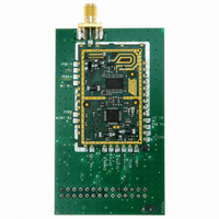
... PCB Layout Design Figure 9-1. PCB Layout ATR2406-DEV-BOARD ATR2406 18 4779N–ISM–12/08 ...
Page 19
... Not necessary if supplied RefClk level is within specification range AUX regulator is used, then T1 and C16 can be removed and a jumper is needed from the collector to the emitter pad. Additionally, pin 7 of the ATR2406 has to be connected to pin 4 or pin 5 to use the integrated F antenna, set jumper R2 (0R resistor 0603) Table 9-2 ...
Page 20
... ATR2406 + AVR internal calculations) 30 µs = 0.93 µAs (charge for configuring the ATR2406) 110 µs = 3.41 µAs (charge for settling the loop filter) 210 µ ...
Page 21
... If the device will be used 1000 times a day Average current in active mode: System Power Down current: Current ATmega88: Current ATR2406: Current VREG (+ ShutDown): Assumed average power-down current is 5 µA. Overall power consumption is 8.1 µ assumed the system uses a small battery with a capacity of 100 mAh. This is 100.000 µAh. ...
Page 22
... Exposed pad 3.7 x 3.7 Dimensions in mm Not indicated tolerances ± 0. Drawing-No.: 6.543-5096.01-4 Issue: 1; 22.01.03 ATR2406 22 Package Remarks QFN32 - 5x5 Taped and reeled, Pb-free – RF module Complete evaluation kit – and reference design ATR2406 + ATmega88 0.9 ±0.1 +0 0.05 -0. MOQ 4000 3 technical drawings ...
Page 23
... Recommended Footprint/Landing Pattern Figure 13-1. Recommenced Footprint/Landing Pattern Table 13-1. 4779N–ISM–12/08 Recommended Footprint/Landing Pattern Signs Sign ATR2406 Size 3.2 mm 1.2 mm 0.3 mm 1.1 mm 0.3 mm 0.2 mm 0. ...
Page 24
... Please note that the following page numbers referred to in this section refer to the specific revision mentioned, not to this document. Revision No. 4779N-ISM-12/08 4779M-ISM-02/07 4779L-ISM-08/06 4779K-ISM-06/06 ATR2406 24 History Put datasheet in a new template Section 12 “Package Information” on page 22 changed Put datasheet in a new template Table 9-1 “Bill of Materials” on page 19 changed Table “ ...
Page 25
... Disclaimer: The information in this document is provided in connection with Atmel products. No license, express or implied, by estoppel or otherwise, to any intellectual property right is granted by this document or in connection with the sale of Atmel products. EXCEPT AS SET FORTH IN ATMEL’S TERMS AND CONDI- TIONS OF SALE LOCATED ON ATMEL’S WEB SITE, ATMEL ASSUMES NO LIABILITY WHATSOEVER AND DISCLAIMS ANY EXPRESS, IMPLIED OR STATUTORY WARRANTY RELATING TO ITS PRODUCTS INCLUDING, BUT NOT LIMITED TO, THE IMPLIED WARRANTY OF MERCHANTABILITY, FITNESS FOR A PARTICULAR PURPOSE, OR NON-INFRINGEMENT ...