UPC8181TB-EVAL NEC, UPC8181TB-EVAL Datasheet
UPC8181TB-EVAL
Specifications of UPC8181TB-EVAL


Related parts for UPC8181TB-EVAL

UPC8181TB-EVAL Summary of contents
Page 1
... HIGH-DENSITY SURFACE MOUNTING: 6-pin super minimold package (2.0 x 1.25 x 0.9 mm) DESCRIPTION NEC's UPC8181TB is a silicon Monolithic Microwave Inte- grated Circuit designed as an amplifier for mobile communica- tions. This IC operates at 3 volts. The medium output power is suitable for RF-TX of mobile communication systems. ...
Page 2
... RATINGS SYMBOLS V 3 Note: mW 270 1. Same voltage applied to pins 4 and 6 -40 to +85 °C -55 to +150 °C dBm +10 (Unless otherwise specified (V) UPC8181TB S06 UNITS MIN TYP dBm +5.5 +8.0 +4.5 +7.0 +4.5 +7.0 dBm – +9.5 – +9.0 – +9.0 dB 4.5 7.5 7 ...
Page 3
... Input Power, P (dBm) IN (Unless otherwise specified 25˚C) A INPUT RETURN LOSS, OUTPUT RETURN LOSS vs. 3.0 +15 +10 -10 -15 -20 -25 -30 0 +10 +12 + +10 UPC8181TB FREQUENCY - 3 -10 RL out -15 0.1 0.3 1.0 3.0 Frequency, f (GHz) OUTPUT POWER vs. INPUT POWER f = 1.9 GHz -50 -40 -30 -20 -10 ...
Page 4
... UPC8181TB TYPICAL PERFORMANCE CURVES THIRD ORDER INTERMODULATION DISTORTION vs. OUTPUT POWER OF EACH TONE 0 - -30 -40 -50 -60 -15 - Output Power of Each Tone, P THIRD ORDER INTERMODULATION DISTORTION vs. OUTPUT POWER OF EACH TONE - -30 -40 -50 -60 -15 - Output Power of Each Tone, P (Unless otherwise specified, T THIRD ORDER INTERMODULATION DISTORTION vs. ...
Page 5
... UPC8181TB 0.1 G 1.0 G 3.0 G 2.0 G 4.0 G S22 S 22 MAG ANG K 0.338 -1.6 1.89 0.346 -2.1 1.73 0.344 -1.0 1.72 0.335 -2 ...
Page 6
... V 2.7 to 3.3 — CC APPLICATION EXAMPLE (Digital Cellular Telephone UPC8181TB = 3 Description Signal input pin. An internal matching circuit, configured with resistors, enables 50 Ω connec- tion over a wide band. A multi- feedback circuit is designed to cancel the deviations of h and FE resistance. This pin must be coupled to signal source with capacitor for DC cut ...
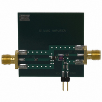
Page 7
... Note: Embossed tape 8 mm wide. Pins 1,2,3 face tape perforation side. APPLICATION BOARD 100 nH 50Ω OUT Note: 1. double sided copper clad GETEK board (H = .028, 2. Back side: GND pattern. 3. Solder plated on patterns Through holes. UPC8181TB (Top View) (Bottom View PACKAGE 6-pin super minimold Si MMIC AMPLIFIER RF OUT L1 C2 ...
Page 8
Subject: Compliance with EU Directives CEL certifies, to its knowledge, that semiconductor and laser products detailed below are compliant with the requirements of European Union (EU) Directive 2002/95/EC Restriction on Use of Hazardous Substances in electrical and electronic equipment (RoHS) ...