RF2312PCK-50 OHM RFMD, RF2312PCK-50 OHM Datasheet
RF2312PCK-50 OHM
Specifications of RF2312PCK-50 OHM


Related parts for RF2312PCK-50 OHM


RF2312PCK-50 OHM Summary of contents
Page 1
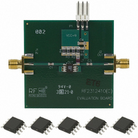
... Package Style: SOIC-8 Linear General Purpose Amplifier Fully Assembled Evaluation Board - 75Ω Fully Assembled Evaluation Board - 50Ω Tel (336) 664 1233 Fax (336) 664 0454 http://www.rfmd.com 3-1 ...
Page 2
RF2312 Absolute Maximum Ratings Parameter Input RF Power Output Load VSWR Ambient Operating Temperature Storage Temperature Parameter Min. Overall (50Ω) Frequency Range Gain 14.5 Noise Figure Input VSWR Output VSWR Output IP 3 Output IP 3 Output IP 3 Output ...
Page 3
Parameter Min. Overall (75Ω) Frequency Range Gain 14.5 Noise Figure Input VSWR Output VSWR Output IP 3 Output IP 3 Output IP 3 Output P 1dB Output P 1dB Output P 1dB Saturated Output Power Saturated Output Power Saturated Output ...
Page 4
RF2312 Parameter Min. Overall (75Ω Push-Pull) Frequency Range Gain Noise Figure Input VSWR Output VSWR Output IP 2 Output IP 3 Second Harmonic 3-4 Specification Unit Typ. Max 150 MHz 15 dB 5.0 dB 1.1:1 1.2:1 +71 dBm ...
Page 5
Pin Function Description input pin. This pin is NOT internally DC-blocked. A DC-blocking capacitor, suitable for the frequency of operation, should be used in all applications. The device has internal feedback, and not using a DC- ...
Page 6
RF2312 5MHz to 50MHz Reverse Path kΩ NOTE 1: Optional resistor R can be used to maintain the correct bias level at higher supply voltages. This is used to S increase output capability ...
Page 7
F EDGE Rev C6 051025 Application Schematic Push-Pull Standard Voltage 120 Ω RF2312 RF2312 RF2312 P1 1 GND 2 3 ...
Page 8
RF2312 2400 Ω 616PT- 1030 F EDGE 10 nF 2400 Ω 120 Ω 3-8 Application Schematic Push-Pull 24V 120 Ω 120 Ω 120 Ω RF2312 10 uH 120 Ω ...
Page 9
... Evaluation Board Schematic - 50Ω (Download Bill of Materials from www.rfmd.com.) P1 H3M P1-1 1 VCC ( GND 220 pF micro strip J1 SMA Evaluation Board Schematic - 75Ω P1-1 VCC 2 GND 3 NC CON3 micro strip F CONN (75 Ω) NOTE: For 5V applications may be removed (shorted). This will result in degraded distortion performance. ...
Page 10
RF2312 Evaluation Board Layout - 50Ω 3-10 2.02” x 2.02” Board Thickness 0.031”, Board Material FR-4 Rev C6 051025 ...
Page 11
Evaluation Board Layout - 75Ω Rev C6 051025 Standard Voltage 1.40” x 1.40” Board Thickness 0.062”, Board Material FR-4 RF2312 3-11 ...
Page 12
RF2312 Evaluation Board Layout - 75Ω 3-12 Push-Pull, Standard Voltage 1.70” x 1.50” Board Thickness 0.062”, Board Material FR-4 Rev C6 051025 ...
Page 13
Evaluation Board Layout - 75Ω Rev C6 051025 Push-Pull, 24V 1.70” x 1.50” Board Thickness 0.062”, Board Material FR-4 RF2312 3-13 ...
Page 14
RF2312 P versus P OUT 500 MHz 20.0 15.0 10.0 5.0 0.0 -15.0 -10.0 -5.0 P (dBm) IN Output Third Order Intercept Point (OIP3) versus P 500 MHz 50.0 40.0 30.0 20.0 10.0 0.0 -15.0 -10.0 -5.0 P (dBm) IN ...
Page 15
CH1 4_: 53.809 -24.182 C2 4 START .300 000 MHz STOP 3 000.000 000 MHz CH1 4_: 19.802 -16.739 START .300 000 MHz STOP 3 000.000 000 ...
Page 16
RF2312 75 Ohms, ICC = 100 mA, Temp = 25°C S[2,2] S[1,1] 3-16 75 Ohms, ICC = 110 mA, Temp = 25°C Swp Max 2.001GHz S[2,2] Swp Min 0.001GHz Swp Max 2.001GHz S[1,1] Swp Min 0.001GHz Rev C6 051025 ...