AD6640AST Analog Devices Inc, AD6640AST Datasheet - Page 2
AD6640AST
Manufacturer Part Number
AD6640AST
Description
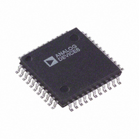
IC ADC 12BIT 65MSPS 44-LQFP
Manufacturer
Analog Devices Inc
Datasheet
1.AD6640STPCB.pdf
(24 pages)
Specifications of AD6640AST
Rohs Status
RoHS non-compliant
Function
A/D Converter
Rf Type
Cellular/PCS, GPS
Secondary Attributes
12 Bit, 65MSPS
Package / Case
44-LQFP
Available stocks
Company
Part Number
Manufacturer
Quantity
Price
Company:

Part Number:
AD6640AST
Manufacturer:
AD
Quantity:
13 888
Company:
Part Number:
AD6640AST
Manufacturer:
ADI
Quantity:
240
Part Number:
AD6640ASTZ
Manufacturer:
ADI/亚德诺
Quantity:
20 000


AD6640–SPECIFICATIONS
DC SPECIFICATIONS
Parameter
RESOLUTION
ACCURACY
TEMPERATURE DRIFT
POWER SUPPLY REJECTION RATIO (PSRR)
REFERENCE OUT (V
ANALOG INPUTS (AIN, AIN)
POWER SUPPLY
POWER CONSUMPTION
NOTES
1
2
3
4
Specifications subject to change without notice
DIGITAL SPECIFICATIONS
Parameter
LOGIC INPUTS (ENCODE, ENCODE)
LOGIC OUTPUTS (D11–D0)
NOTES
1
2
3
4
Specifications subject to change without notice.
The AD6640 is designed to be driven differentially. Both AIN and AIN should be driven at levels V
Best dynamic performance is obtained by driving ENCODE and ENCODE differentially. See Encoding the AD6640 section for more details. Performance versus ENCODE/ENCODE
For dc-coupled applications, the ENCODE input common-mode range specifies the common-mode range the ENCODE inputs can tolerate when driven differentially by the
ENCODE or ENCODE may be driven alone if desired, but performance will likely be degraded. Logic compatibility specifications are provided to show that TTL or CMOS
Digital output load is one LCX gate.
ENCODE = 20 MSPS
If V
a 2 V p-p differential input signal. See Driving the Analog Inputs section for more details.
Analog input common-mode range specifies the offset range the analog inputs can tolerate in dc-coupled applications (see Figure 17 for more detail).
power is shown in TPC 12.
minimum differential input voltage of 0.4 V p-p. For differential input voltage swings greater than 0.4 V p-p, the common-mode range will change. The minimum value ensures
that the input voltage on either encode pin does not go below 0 V. The maximum value ensures that the input voltage on either ENCODE pin does not go below 2.0 V or above
AV
clock sources will work. When driving only one ENCODE input, bypass the complementary input to GND with 0.01 µF.
No Missing Codes
Offset Error
Gain Error
Differential Nonlinearity (DNL)
Integral Nonlinearity (INL)
Offset Error
Gain Error
Analog Input Common-Mode Range
Differential Input Voltage Range
Differential Input Resistance
Differential Input Capacitance
Supply Voltage
Supply Current
ENCODE Input Common-Mode Range
Differential Input Voltage
Single-Ended ENCODE
Input Capacitance
Logic Compatibility
Logic “1” Voltage (DV
Logic “0” Voltage (DV
Logic “1” Voltage (DV
Logic “0” Voltage (DV
Output Coding
CC
REF
AV
DV
IA
ID
Logic Compatibility
Logic “1” Voltage
Logic “0” Voltage
Logic “1” Current (V
Logic “0” Current (V
(e.g., for a differential input swing of 0.8 V, the min and max common-mode specs become 0.4 V and 2.4 V, respectively).
VCC
is used to provide a dc offset to other circuits, it should first be buffered.
VCC
CC
CC
(AV
(DV
CC
CC
= 5.0 V)
= 3.3 V)
REF
3
CC
CC
CC
CC
INH
INL
)
2
= 3.3 V)
= 3.3 V)
= 5.0 V)
= 5.0 V)
1
= 0 V)
= 5 V)
4
3
1
(AV
CC
.
4
= 5 V, DV
1
2
(AV
CC
= 5 V, DV
CC
= 3.3 V; T
CC
Temp
+25°C
Full
Full
+25°C
Full
Full
Full
Full
Full
Full
Full
Full
+25°C
Full
Full
Full
Full
Full
Temp
Full
Full
Full
Full
Full
Full
+25°C
Full
Full
Full
Full
= 3.3 V; T
MIN
= –40 C, T
–2–
MIN
Test
Level
I
VI
VI
I
V
V
V
V
V
V
V
IV
V
VI
VI
VI
VI
VI
Test
Level
IV
IV
VI
VI
VI
VI
V
VI
VI
IV
IV
= –40 C, T
MAX
= +85 C, unless otherwise noted.)
REF
± 0.5 V. The input signals should be 180 degrees out of phase to produce
MAX
Min
–10
–10
–1.0
0.7
4.75
3.0
Min
0.2
0.4
2.0
0
+500
–400
2.8
4.5
= +85 C, unless otherwise noted.)
Twos Complement
GUARANTEED
AD6640AST
AD6640AST
TTL/CMOS
CMOS
Typ
12
+3.5
+4.0
± 0.5
± 1.25
50
100
± 0.5
2.4
V
2.0
0.9
1.5
5.0
3.3
135
10
710
Typ
+650
–320
2.5
DV
0.2
DV
0.35
REF
CC
CC
± 0.05
– 0.2
– 0.3
Max
+10
+10
+1.5
1.1
5.25
5.25
160
20
865
Max
2.2
10
5.0
0.8
+800
–200
0.5
0.5
Unit
Bits
mV
% FS
LSB
LSB
ppm/°C
ppm/°C
mV/V
V
V
V p-p
pF
V
V
mA
mA
mW
Unit
V
V p-p
V p-p
V
µA
µA
pF
V
V
V
V
kΩ
V
REV. A
Related parts for AD6640AST
Image
Part Number
Description
Manufacturer
Datasheet
Request
R

Part Number:
Description:
±1.7g Dual-Axis IMEMS Accelerometer Evaluation Board
Manufacturer:
Analog Devices Inc
Datasheet:

Part Number:
Description:
Inertial Sensor Evaluation System
Manufacturer:
Analog Devices Inc
Datasheet:
Part Number:
Description:
Manufacturer:
Analog Devices Inc
Datasheet:
Part Number:
Description:
Manufacturer:
Analog Devices Inc
Datasheet:
Part Number:
Description:
Manufacturer:
Analog Devices Inc
Datasheet:
Part Number:
Description:
Manufacturer:
Analog Devices Inc
Datasheet:
Part Number:
Description:
Manufacturer:
Analog Devices Inc
Datasheet:
Part Number:
Description:
Manufacturer:
Analog Devices Inc
Datasheet:
Part Number:
Description:
Manufacturer:
Analog Devices Inc
Datasheet:
Part Number:
Description:
Manufacturer:
Analog Devices Inc
Datasheet:
Part Number:
Description:
Manufacturer:
Analog Devices Inc
Datasheet:
Part Number:
Description:
Manufacturer:
Analog Devices Inc
Datasheet:
Part Number:
Description:
Manufacturer:
Analog Devices Inc
Datasheet: