RXD-433-KH2 Linx Technologies Inc, RXD-433-KH2 Datasheet - Page 2
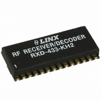
RXD-433-KH2
Manufacturer Part Number
RXD-433-KH2
Description
RECEIVER/DECODER 433MHZ KH2 SER
Manufacturer
Linx Technologies Inc
Series
KH2r
Datasheet
1.RXD-418-KH2.pdf
(11 pages)
Specifications of RXD-433-KH2
Frequency
433MHz
Sensitivity
-102dBm
Data Rate - Maximum
5 kbps
Modulation Or Protocol
ASK, OOK
Applications
Garage Openers, RKE, Security Alarms
Current - Receiving
5mA
Data Interface
PCB, Surface Mount
Antenna Connector
PCB, Surface Mount
Features
Built-in Remote Control Decoder
Voltage - Supply
2.7 V ~ 3.6 V
Operating Temperature
-40°C ~ 70°C
Package / Case
Non-Standard SMD
Board Size
36.3 mm x 16 mm x 4.6 mm
Minimum Operating Temperature
- 40 C
Supply Voltage (min)
2.7 V
Product
RF Modules
Maximum Frequency
433.92 MHz
Supply Voltage (max)
3.6 V
Maximum Operating Temperature
+ 70 C
Lead Free Status / RoHS Status
Lead free / RoHS Compliant
Memory Size
-
Lead Free Status / Rohs Status
Lead free / RoHS Compliant
Available stocks
Company
Part Number
Manufacturer
Quantity
Price
Company:

Part Number:
RXD-433-KH2
Manufacturer:
LNX
Quantity:
100


Table 1: KH2 Series Receiver Specifications
Notes
1. The KH2 can utilize a 4.3 to 5.2VDC supply provided a 330-ohm resistor is placed in series with VCC.
2. Into a 50-ohm load.
3. When operating from a 5V source, it is important to consider that the output will swing to well less than
4. For BER of 10 -5 at 1,200bps.
5. Characterized, but not tested.
6. Time to valid data output.
7. Maximum drive capability of data outputs.
Page 2
ELECTRICAL SPECIFICATIONS
Parameter
POWER SUPPLY
Operating Voltage
Supply Current
Power-Down Current
RECEIVER SECTION
Receive Frequency Range:
Center Frequency Accuracy
LO Feedthrough
IF Frequency
Noise Bandwidth
Data Rate
Data Output:
Power-Down Input:
Receiver Sensitivity
RSSI / Analog:
ANTENNA PORT
RF Input Impedance
TIMING
Receiver Turn-On Time:
Max. Time Between Transitions
DECODER SECTION
TX Data Length
Average Data Duty Cycle
Decoder Oscillator
Output Drive Current
ENVIRONMENTAL
Operating Temperature Range
RXD-315-KH2
RXD-418-KH2
RXD-433-KH2
Logic Low
Logic High
Logic Low
Logic High
Dynamic Range
Analog Bandwidth
Gain
Voltage With No Carrier
Via V
Via PDN
5 volts as a result of the required dropping resistor. Please verify that the minimum voltage will meet the
high threshold requirement of the device to which data is being sent.
With Dropping Resistor
CC
Designation
N
F
V
I
V
V
R
I
PDN
F
V
V
F
CC
ENC
–
–
3DB
–
–
–
–
–
–
–
–
–
–
–
–
–
CC
OL
OH
IH
C
IF
IL
IN
V
CC
Min.
20.0
-106
0.04
100
2.7
4.3
4.0
-50
3.0
0.6
-40
50
–
–
–
–
–
–
–
–
–
–
–
–
–
–
–
–
–
-0.4
26 bits 3x
Typical
433.92
28.0
10.7
-112
0.25
10.0
50%
315
418
280
3.0
5.0
5.2
-80
0.0
3.0
1.5
7.0
1.0
80
16
50
70
–
–
–
–
–
–
10,000
5,000
Max.
35.0
-118
10.0
0.50
+50
+70
3.6
5.2
7.0
0.4
1.2
–
–
–
–
–
–
–
–
–
–
–
–
–
–
–
–
–
mV / dB
Units
mSec
mSec
mSec
VDC
VDC
MHz
MHz
MHz
dBm
MHz
VDC
VDC
VDC
VDC
dBm
kHz
kHz
kHz
mA
bps
mA
µA
dB
Hz
°
V
Ω
–
–
C
Notes
1,5
2,5
5,6
5,6
–
–
5
–
–
–
–
5
–
–
3
3
–
–
4
5
5
5
5
5
5
–
–
–
7
5
ABSOLUTE MAXIMUM RATINGS
PERFORMANCE DATA
TYPICAL PERFORMANCE GRAPHS
Figure 3: Turn-On Time from V
Figure 5: Consumption vs. Supply
5.40
5.35
5.30
5.25
5.20
5.15
5.10
2.7 2.8 2.9
These performance parameters
are based on module operation at
25°C from a 3.0VDC supply unless
otherwise
illustrates
necessary
operation. It is recommended all
ground pins be connected to the
ground plane. The pins marked NC
have no electrical connection and
are designed only to add physical
support.
3.0 3.1 3.2 3.3
Supply Voltage V
Supply Voltage V
Any Input or Output Pin
RF Input
Operating Temperature
Storage Temperature
Soldering Temperature
*NOTE*
damage to the device. Furthermore, extended operation at these maximum
ratings may reduce the life of this device.
Supply
3.4 3.5 3.6 3.7
Exceeding any of the limits of this section may lead to permanent
RX Data
3.8 3.9 4.0 4.1 4.2 4.3 4.4 4.5
noted.
Supply Voltage (VDC)
for
the
testing
With Dropping
CC
CC
Resistor
connections
CC
, Using Resistor
Figure
4.6 4.7 4.8 4.9
5.0 5.1 5.2
and
2
Figure 2: Test / Basic Application Circuit
Figure 4: Turn-On Time from PDN
Figure 6: RSSI Response Time
-0.3
-0.3
-0.3
External
Resistor
-30
-45
330Ω
NO RFIN
+225°C for 10 seconds
5VDC
PDN
3VDC
to
to
to
to
to
0
10
11
12
13
14
1
2
3
4
5
6
7
8
9
RX DATA
RFIN >-35dBm
NC
D0
D1
GND
VCC
PDN
D2
D3
D4
DATA
VT
D5
D6
D7
+3.6
+5.2
+3.6
+70
+85
GND
RSSI
ANT
NC
A9
A8
A7
A6
A5
A4
A3
A2
A1
A0
VDC
VDC
VDC
dBm
°C
°C
28
27
26
25
24
23
22
21
20
19
18
17
16
15
Page 3
Related parts for RXD-433-KH2
Image
Part Number
Description
Manufacturer
Datasheet
Request
R

Part Number:
Description:
RECEIVER RF 433MHZ SMT
Manufacturer:
Linx Technologies Inc
Datasheet:

Part Number:
Description:
RECEIVER RF 418MHZ SMT KH2 SER
Manufacturer:
Linx Technologies Inc
Datasheet:

Part Number:
Description:
RECEIVER RF 315MHZ SMT KH2 SER
Manufacturer:
Linx Technologies Inc
Datasheet:

Part Number:
Description:
RECEIVER RF 315MHZ SMT
Manufacturer:
Linx Technologies Inc
Datasheet:
Part Number:
Description:
RECEIVER RF 418MHZ SMT
Manufacturer:
Linx Technologies Inc
Datasheet:

Part Number:
Description:
HOLDER BATTERY 20MM COIN CR2032
Manufacturer:
Linx Technologies Inc
Datasheet:

Part Number:
Description:
CONN RPSMA BL CRJA-CPV 8.5" COAX
Manufacturer:
Linx Technologies Inc

Part Number:
Description:
CABLE RG174 RPSMA M/F 8.5"
Manufacturer:
Linx Technologies Inc

Part Number:
Description:
CABLE RG174 SMA M/F 8.5"
Manufacturer:
Linx Technologies Inc

Part Number:
Description:
CABLE RPSMA/SMA 8.5"
Manufacturer:
Linx Technologies Inc

Part Number:
Description:
MODULE USB LOW SPEED
Manufacturer:
Linx Technologies Inc
Datasheet:

Part Number:
Description:
IC TRANSCODER MT BI-DIR 20-SSOP
Manufacturer:
Linx Technologies Inc
Datasheet:

Part Number:
Description:
IC ENCODER LOW SECURITY 8DIP
Manufacturer:
Linx Technologies Inc
Datasheet:

Part Number:
Description:
IC DECODER MS SERIES 20-SSOP
Manufacturer:
Linx Technologies Inc
Datasheet:
Part Number:
Description:
IC ENCODER MS SERIES 20-SSOP
Manufacturer:
Linx Technologies Inc
Datasheet: