RXD-433-KH2 Linx Technologies Inc, RXD-433-KH2 Datasheet - Page 6
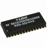
RXD-433-KH2
Manufacturer Part Number
RXD-433-KH2
Description
RECEIVER/DECODER 433MHZ KH2 SER
Manufacturer
Linx Technologies Inc
Series
KH2r
Datasheet
1.RXD-418-KH2.pdf
(11 pages)
Specifications of RXD-433-KH2
Frequency
433MHz
Sensitivity
-102dBm
Data Rate - Maximum
5 kbps
Modulation Or Protocol
ASK, OOK
Applications
Garage Openers, RKE, Security Alarms
Current - Receiving
5mA
Data Interface
PCB, Surface Mount
Antenna Connector
PCB, Surface Mount
Features
Built-in Remote Control Decoder
Voltage - Supply
2.7 V ~ 3.6 V
Operating Temperature
-40°C ~ 70°C
Package / Case
Non-Standard SMD
Board Size
36.3 mm x 16 mm x 4.6 mm
Minimum Operating Temperature
- 40 C
Supply Voltage (min)
2.7 V
Product
RF Modules
Maximum Frequency
433.92 MHz
Supply Voltage (max)
3.6 V
Maximum Operating Temperature
+ 70 C
Lead Free Status / RoHS Status
Lead free / RoHS Compliant
Memory Size
-
Lead Free Status / Rohs Status
Lead free / RoHS Compliant
Available stocks
Company
Part Number
Manufacturer
Quantity
Price
Company:

Part Number:
RXD-433-KH2
Manufacturer:
LNX
Quantity:
100


BOARD LAYOUT GUIDELINES
Page 10
If you are at all familiar with RF devices, you may be concerned about
specialized board layout requirements. Fortunately, because of the care taken by
Linx in designing the modules, integrating them is very straightforward. Despite
this ease of application, it is still necessary to maintain respect for the RF stage
and exercise appropriate care in layout and application in order to maximize
performance and ensure reliable operation. The antenna can also be influenced
by layout choices. Please review this data guide in its entirety prior to beginning
your design. By adhering to good layout principles and observing some basic
design rules, you will be on the path to RF success.
The adjacent figure shows the suggested
PCB footprint for the module. The actual pad
dimensions are shown in the Pad Layout
section of this manual. A ground plane (as
large as possible) should be placed on a
lower layer of your PC board opposite the
module. This ground plane can also be critical
to the performance of your antenna, which will
be discussed later. There should not be any
ground or traces under the module on the
same layer as the module, just bare PCB.
During prototyping, the module should be soldered to a properly laid-out circuit
board. The use of prototyping or “perf” boards will result in horrible performance
and is strongly discouraged.
No conductive items should be placed within 0.15in of the module’s top or sides.
Do not route PCB traces directly under the module. The underside of the module
has numerous signal-bearing traces and vias that could short or couple to traces
on the product’s circuit board.
The module’s ground lines should each have their own via to the ground plane
and be as short as possible.
AM / OOK receivers are particularly subject to noise. The module should, as
much as reasonably possible, be isolated from other components on your PCB,
especially high-frequency circuitry such as crystal oscillators, switching power
supplies, and high-speed bus lines. Make sure internal wiring is routed away
from the module and antenna, and is secured to prevent displacement.
The power supply filter should be placed close to the module’s V
In some instances, a designer may wish to encapsulate or “pot” the product.
Many Linx customers have done this successfully; however, there are a wide
variety of potting compounds with varying dielectric properties. Since such
compounds can considerably impact RF performance, it is the responsibility of
the designer to carefully evaluate and qualify the impact and suitability of such
materials.
The trace from the module to the antenna should be kept as short as possible.
A simple trace is suitable for runs up to 1/8-inch for antennas with wide
bandwidth characteristics. For longer runs or to avoid detuning narrow bandwidth
antennas, such as a helical, use a 50-ohm coax or 50-ohm microstrip
transmission line as described in the following section.
Figure 15: Suggested PCB Layout
GROUND PLANE
GROUND PLANE
GROUND PLANE
ON LOWER LAYER
ON LOWER LAYER
ON LOWER LAYER
CC
line.
MICROSTRIP DETAILS
Figure 16: Microstrip Formulas
Dielectric Constant Width/Height (W/d)
A transmission line is a medium whereby RF energy is transferred from one
place to another with minimal loss. This is a critical factor, especially in high-
frequency products like Linx RF modules, because the trace leading to the
module’s antenna can effectively contribute to the length of the antenna,
changing its resonant bandwidth. In order to minimize loss and detuning, some
form of transmission line between the antenna and the module should be used,
unless the antenna can be placed very close (<1/8in.) to the module. One
common form of transmission line is a coax cable, another is the microstrip. This
term refers to a PCB trace running over a ground plane that is designed to serve
as a transmission line between the module and the antenna. The width is based
on the desired characteristic impedance of the line, the thickness of the PCB,
and the dielectric constant of the board material. For standard 0.062in thick FR-
4 board material, the trace width would be 111 mils. The correct trace width can
be calculated for other widths and materials using the information below. Handy
software for calculating microstrip lines is also available on the Linx website,
www.linxtechnologies.com.
4.80
4.00
2.55
1.8
2.0
3.0
Effective Dielectric
Constant
3.59
3.07
2.12
Trace
Characteristic
Ground plane
Impedance
50.0
51.0
48.0
Board
Page 11
Related parts for RXD-433-KH2
Image
Part Number
Description
Manufacturer
Datasheet
Request
R

Part Number:
Description:
RECEIVER RF 433MHZ SMT
Manufacturer:
Linx Technologies Inc
Datasheet:

Part Number:
Description:
RECEIVER RF 418MHZ SMT KH2 SER
Manufacturer:
Linx Technologies Inc
Datasheet:

Part Number:
Description:
RECEIVER RF 315MHZ SMT KH2 SER
Manufacturer:
Linx Technologies Inc
Datasheet:

Part Number:
Description:
RECEIVER RF 315MHZ SMT
Manufacturer:
Linx Technologies Inc
Datasheet:
Part Number:
Description:
RECEIVER RF 418MHZ SMT
Manufacturer:
Linx Technologies Inc
Datasheet:

Part Number:
Description:
HOLDER BATTERY 20MM COIN CR2032
Manufacturer:
Linx Technologies Inc
Datasheet:

Part Number:
Description:
CONN RPSMA BL CRJA-CPV 8.5" COAX
Manufacturer:
Linx Technologies Inc

Part Number:
Description:
CABLE RG174 RPSMA M/F 8.5"
Manufacturer:
Linx Technologies Inc

Part Number:
Description:
CABLE RG174 SMA M/F 8.5"
Manufacturer:
Linx Technologies Inc

Part Number:
Description:
CABLE RPSMA/SMA 8.5"
Manufacturer:
Linx Technologies Inc

Part Number:
Description:
MODULE USB LOW SPEED
Manufacturer:
Linx Technologies Inc
Datasheet:

Part Number:
Description:
IC TRANSCODER MT BI-DIR 20-SSOP
Manufacturer:
Linx Technologies Inc
Datasheet:

Part Number:
Description:
IC ENCODER LOW SECURITY 8DIP
Manufacturer:
Linx Technologies Inc
Datasheet:

Part Number:
Description:
IC DECODER MS SERIES 20-SSOP
Manufacturer:
Linx Technologies Inc
Datasheet:
Part Number:
Description:
IC ENCODER MS SERIES 20-SSOP
Manufacturer:
Linx Technologies Inc
Datasheet: