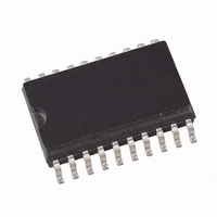
ATA8204P3-TKQY Atmel, ATA8204P3-TKQY Datasheet - Page 15

ATA8204P3-TKQY
Manufacturer Part Number
ATA8204P3-TKQY
Description
IC RCVR ASK/FSK UHF 433MHZ 20SSO
Manufacturer
Atmel
Datasheet
1.ATA8203P3-TKQY.pdf
(46 pages)
Specifications of ATA8204P3-TKQY
Frequency
433MHz
Sensitivity
-115dBm
Data Rate - Maximum
10 kbps
Modulation Or Protocol
ASK, FSK
Applications
General Purpose
Current - Receiving
8.5mA
Data Interface
PCB, Surface Mount
Antenna Connector
PCB, Surface Mount
Features
RSSI Equipped
Voltage - Supply
4.5 V ~ 5.5 V
Operating Temperature
-40°C ~ 85°C
Package / Case
20-SOIC (0.200", 5.30mm Width)
Pin Count
20
Screening Level
Industrial
Lead Free Status / RoHS Status
Lead free / RoHS Compliant
Memory Size
-
Lead Free Status / Rohs Status
Compliant
Figure 8-5.
Figure 8-6.
8.4
8.5
9121B–INDCO–04/09
Duration of the Bit Check
Receiving Mode
(Lim_min = 14, Lim_max = 24)
(Lim_min = 14, Lim_max = 24)
IC_ACTIVE
IC_ACTIVE
Bit-check
Bit-check
Bit check
Dem_out
Bit check
Dem_out
counter
counter
Timing Diagram for Failed Bit Check (Condition: CV_Lim < Lim_min)
Timing Diagram for Failed Bit Check (Condition: CV_Lim
Start-up mode
Start-up mode
T
T
Start-up
Start-up
If no transmitter signal is present during the bit check, the output of the ASK/FSK demodulator
delivers random signals. The bit check is a statistical process and T
Therefore, an average value for T
depends on the selected baud-rate range and on T
value for T
In the presence of a valid transmitter signal, T
nal, f
a longer period for T
If the bit check was successful for all bits specified by N
mode. According to
that case, and the data clock is available after the start bit has been detected (see
page
the data clock at pin DATA_CLK. The receiver stays in that condition until it is switched back to
polling mode explicitly.
0
0
Sig
20). A connected microcontroller can be woken up by the negative edge at pin DATA or by
, and the count of the checked bits, N
1 2
1 2
Bit-check
3 4
3 4
5 6
5 6
resulting in a lower current consumption in polling mode.
1
7 1
Bit-check mode
Bit-check
Figure 8-2 on page
2 3
T
Bit-check
2 3
4 5
Bit check failed (CV_Lim_ < Lim_min)
4 5
1/2 Bit
requiring a higher value for the transmitter pre-burst T
6 7
Bit-check mode
6 7
8
T
Bit-check
8
9 10
9 10
Bit-check
11 12
1/2 Bit
11 12
13, the internal data signal is switched to pin DATA in
ATA8203/ATA8204/ATA8205
13 14
is given in the electrical characteristics. T
Bit-check
15 16
Bit-check
Lim_max)
Bit check failed (CV_Lim >= Lim_max)
17 18
. A higher value for N
Clk
Sleep mode
19 20
. A higher baud-rate range causes a lower
is dependent on the frequency of that sig-
T
Sleep
Bit-check
0
21 22
23 24
, the receiver switches to receiving
Bit-check
Sleep mode
Bit-check
T
varies for each check.
Sleep
0
thereby results in
Preburst
Figure 9-1 on
.
Bit-check
15


