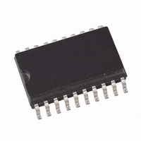
ATA8204P3-TKQY Atmel, ATA8204P3-TKQY Datasheet - Page 23

ATA8204P3-TKQY
Manufacturer Part Number
ATA8204P3-TKQY
Description
IC RCVR ASK/FSK UHF 433MHZ 20SSO
Manufacturer
Atmel
Datasheet
1.ATA8203P3-TKQY.pdf
(46 pages)
Specifications of ATA8204P3-TKQY
Frequency
433MHz
Sensitivity
-115dBm
Data Rate - Maximum
10 kbps
Modulation Or Protocol
ASK, FSK
Applications
General Purpose
Current - Receiving
8.5mA
Data Interface
PCB, Surface Mount
Antenna Connector
PCB, Surface Mount
Features
RSSI Equipped
Voltage - Supply
4.5 V ~ 5.5 V
Operating Temperature
-40°C ~ 85°C
Package / Case
20-SOIC (0.200", 5.30mm Width)
Pin Count
20
Screening Level
Industrial
Lead Free Status / RoHS Status
Lead free / RoHS Compliant
Memory Size
-
Lead Free Status / Rohs Status
Compliant
10. Digital Noise Suppression
10.1
Figure 10-1. Output of Digital Noise at the End of the Data Stream
Figure 10-2. Automatic Noise Suppression
9121B–INDCO–04/09
Automatic Noise Suppression
Data_out (DATA)
Data_out (DATA)
DATA_CLK
DATA_CLK
Bit-check
Bit-check
mode
mode
After a data transmission, digital noise appears on the data output (see
Digital Noise at the End of the Data Stream”). To prevent digital noise keeping the connected
microcontroller busy, it can be suppressed in two different ways:
The receiver changes to bit-check mode at the end of a valid data stream if the bit
Noise_Disable
noise is suppressed, and the level at pin DATA is high. The receiver changes back to receiving
mode, if the bit check was successful.
This method of noise suppression is recommended if the data stream is Manchester or Bi-phase
coded and is active after power on.
Figure 10-3
data output at the end of a data stream. If the last period of the data stream is a high period (ris-
ing edge to falling edge), a pulse occurs on pin DATA. The length of the pulse depends on the
selected baud-rate range.
Bit check ok
Bit check ok
• Automatic Noise Suppression
• Controlled Noise Suppression by the Microcontroller
Preburst
Preburst
data clock control
data clock control
Receiving mode,
Receiving mode,
logic active
logic active
“Occurrence of a Pulse at the End of the Data Stream” illustrates the behavior of the
(Table 11-9 on page
Data
Data
Digital Noise
Receiving mode,
bit check active
Bit-check
27) in the OPMODE register is set to 1 (default). The digital
mode
Digital Noise
ATA8203/ATA8204/ATA8205
Bit check ok
Bit check ok
Preburst
Preburst
data clock control
data clock control
Receiving mode,
Receiving mode,
logic active
logic active
Data
Data
Figure 10-1
Receiving mode,
bit check active
Digital Noise
Bit-check
mode
“Output of
23


