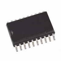
ATA5744N-TKSY Atmel, ATA5744N-TKSY Datasheet

ATA5744N-TKSY
Specifications of ATA5744N-TKSY
Related parts for ATA5744N-TKSY
ATA5744N-TKSY Summary of contents
Page 1
Features • Minimal External Circuitry Requirements Components on the PC Board Except Matching to the Receiver Antenna • High Sensitivity, Especially at Low Data Rates • SSO20 and SO20 package • Fully Integrated VCO • Supply Voltage 4.5V ...
Page 2
Pin Configuration Figure 2-1. Pinning SO20 and SSO20 Table 2-1. Pin Description Pin Symbol 1 BR_0 2 BR_1 3 CDEM 4 AVCC 5 AGND 6 DGND 7 MIXVCC 8 LNAGND 9 LNA_IN LFVCC ...
Page 3
Figure 2-2. Block Diagram CDEM RSSI AVCC AGND DGND MIXVCC LNAGND LNA_IN 3. RF Front End The RF front end of the receiver is a heterodyne configuration that converts the input signal into a 1-MHz IF signal. According to fier), ...
Page 4
Figure 3-1. The passive loop filter connected to pin LF is designed for a loop bandwidth of B This value for B the appropriate loop filter components to achieve the desired loop bandwidth f is determined by the RF input ...
Page 5
Figure 3-2 using a SAW. input matching networks shown in parameters given in the electrical characteristics. Table 3-1. Calculation of LO and IF Frequency Conditions f = 315 MHz, MODE = 433.92 MHz, MODE = 1 ...
Page 6
Figure 3-3. Input Matching Network without SAW Filter f = 433.92 MHz RF C3 25n 15p RF IN 3.3p 100p TOKO LL2012 22n F22NJ Please note that for all coupling conditions (see wire inductivity of the LNA ground is compensated. ...
Page 7
Pin RSSI The output voltage of the RSSI amplifier (VRSSI) is available at pin RSSI. Using the RSSI output signal, the signal strength of different transmitters can be distinguished. The usable input power range P Ref Since different RF ...
Page 8
Table 4-1. Each BR_Range is defined by a minimum and a maximum edge-to-edge time (tee_sig). These limits are defined in the electrical characteristics. They should not be exceeded to maintain full sensitivity of the receiver. 4.5 Receiving Characteristics The RF ...
Page 9
Basic Clock Cycle of the Digital Circuitry The complete timing of the digital circuitry and the analog filtering is derived from one clock. According to bination with a divider. The division factor is controlled by the logical state at ...
Page 10
Pin ENABLE Via the pin ENABLE the operating mode of the receiver can be selected (see ure 5-2). If the pin ENABLE is held to Low, the receiver remains in sleep mode. All circuits for signal pro- cessing are ...
Page 11
Digital Signal Processing The data from the ASK demodulator (Dem_out) is digitally processed in different ways and as a result converted into the output signal DATA. This processing depends on the selected baudrate range (BR_Range). extended basic clock cycle ...
Page 12
Absolute Maximum Ratings Stresses beyond those listed under “Absolute Maximum Ratings” may cause permanent damage to the device. This is a stress rating only and functional operation of the device at these or any other conditions beyond those indicated ...
Page 13
Electrical Characteristics All parameters refer to GND –40°C to +105°C, V amb ( 25°C) S amb Parameters Test Conditions Symbol Basic Clock Cycle of the Digital Circuitry MODE = 0 (USA) Basic clock ...
Page 14
Electrical Characteristics (continued) Parameters Test Conditions Input matched according compression point Figure 3-3 on page (LNA, mixer, IF amplifier Input matched according to Maximum input level Figure 3-3 on page Local Oscillator Operating frequency ...
Page 15
Electrical Characteristics (continued) Parameters Test Conditions Sensitivity variation for full f = 433.92 MHz/ 315 MHz in operating range including 0.79 MHz to 1.21 MHz IF filter compared 0.73 MHz to 1.27 MHz ...
Page 16
Figure 10-1. Application Circuit 2 10% 10% GND C13 C3 5% np0 COAX C17 3 np0 L2 Figure 10-2. Application Circuit ...
Page 17
Figure 10-3. Application Circuit 2 10% 10% GND C13 C3 5% np0 COAX 8 Figure 10-4. Application Circuit ...
Page 18
... Ordering Information Extended Type Number ATA5744N-TKSY ATA5744N-TKQY ATA5744N-TGSY ATA5744N-TGQY 12. Package Information Package SO20 Dimensions in mm 0.4 1. ATA5744 18 Package Remarks SSO20 Tube, Pb-free SSO20 Taped and reeled, Pb-free SO20 Tube, Pb-free SO20 Taped and reeled, Pb-free 12.95 12.70 2.35 0.25 0.10 11.43 ...
Page 19
Package SSO20 Dimensions in mm 0.25 0. 4893A–RKE–11/05 6.75 6.50 1.30 0.15 0.05 5.85 11 technical drawings according to DIN specifications 10 ATA5744 5.7 5.3 4.5 4.3 0.15 6.6 6.3 19 ...
Page 20
... Disclaimer: The information in this document is provided in connection with Atmel products. No license, express or implied, by estoppel or otherwise, to any intellectual property right is granted by this document or in connection with the sale of Atmel products. EXCEPT AS SET FORTH IN ATMEL’S TERMS AND CONDI- TIONS OF SALE LOCATED ON ATMEL’S WEB SITE, ATMEL ASSUMES NO LIABILITY WHATSOEVER AND DISCLAIMS ANY EXPRESS, IMPLIED OR STATUTORY WARRANTY RELATING TO ITS PRODUCTS INCLUDING, BUT NOT LIMITED TO, THE IMPLIED WARRANTY OF MERCHANTABILITY, FITNESS FOR A PARTICULAR PURPOSE, OR NON-INFRINGEMENT ...


